Scanning Acoustic Microscopy (SAM) uses ultrasonic waves to inspect samples for defects, quality issues, and counterfeit components. It works by analyzing the reflection of sound waves to create detailed images of a product’s internal structure without damaging it. SAM is safer for operators than X-ray inspection and can provide high-resolution images of multiple layers within a product.
Scanning Acoustic Microscope designed by Hiwave
Hiwave created SAM systems to meet customer needs. Our products feature advanced software-driven tools with a flexible, modular design. This allows us to serve startups, growing test labs, electronics distributors, semiconductor designers, and production facilities with tailored SAM solutions. Our vertically integrated approach enables us to offer flexible options that fit specific customer requirements.
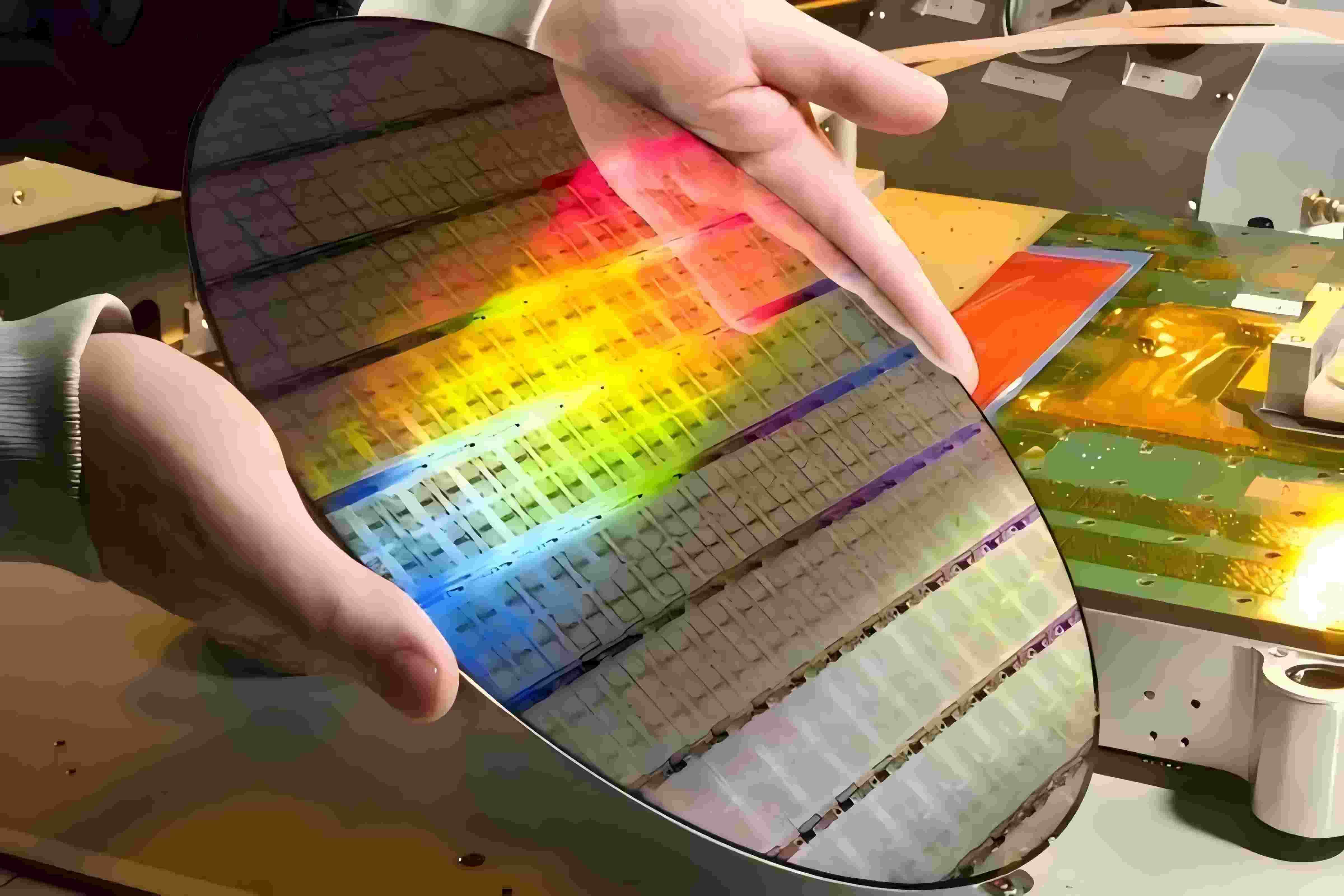
The application of scanning acoustic microscope in semiconductor
Scanning Acoustic Microscopy is vital for inspecting chip packaging, detecting hidden defects like cracks and voids. It ensures reliability, improves quality control, and reduces failure risks in electronics.
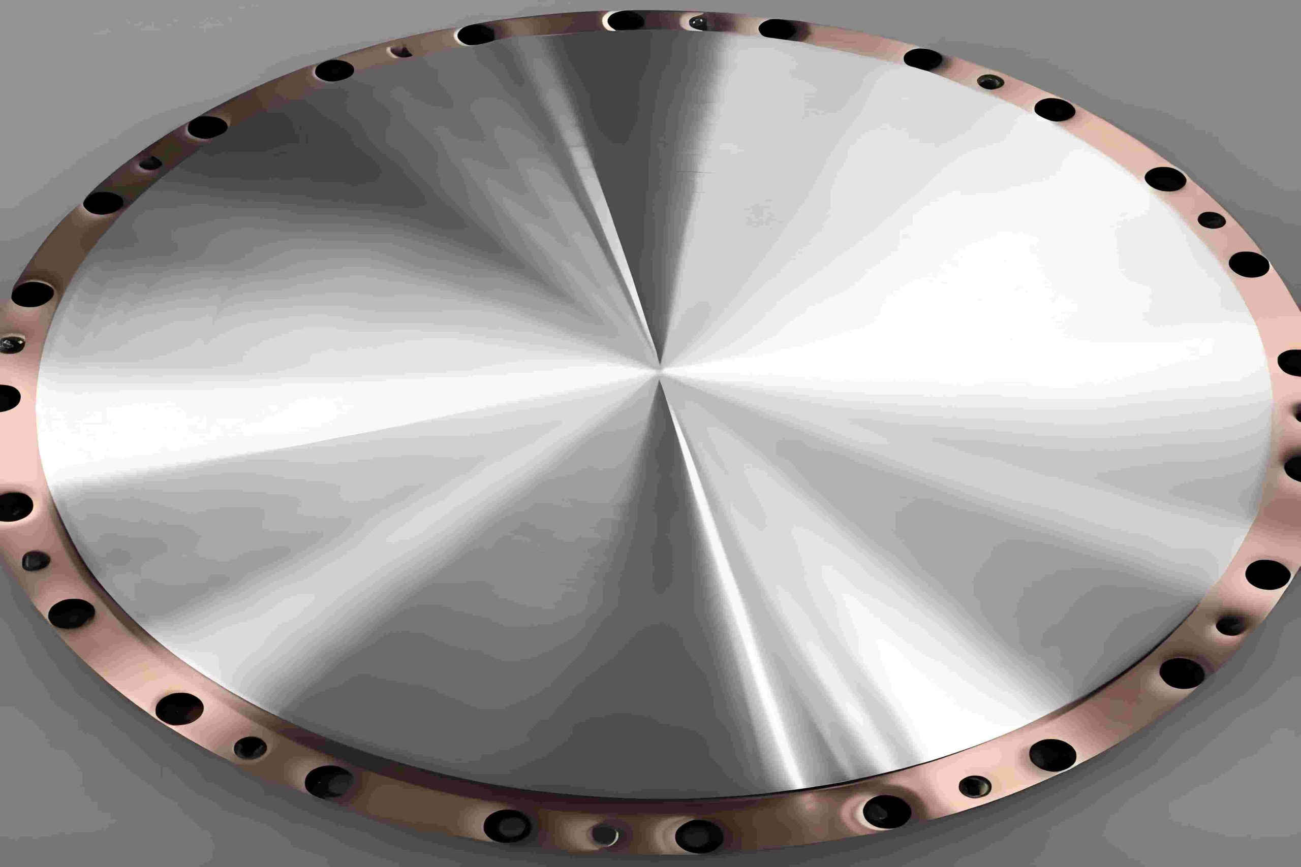
Scanning Acoustic Microscopy is vital for inspecting classic chucks, providing precise, non-destructive defect detection to ensure quality and reliability.