The scanning acoustic microscope (SAM) is based on ultrasonic pulse echo technology. A specific ultrasonic acoustic component emits and receives short ultrasonic pulses with a high repetition rate. After the ultrasonic wave interacts with the sample under test, the reflected wave is received and converted into an electrical signal. The scanning mechanism performs a reciprocating scanning motion on the sample, collects and records the sample’s reflected wave signal intensity and phase information point by point, and then converts the sample structure into a scanned image in the form of grayscale values. Unlike other detection methods such as optics, electron beams, and X-rays, the scanning image of the ultrasonic scanning microscope has high resolution and complete information and is widely used in failure analysis, reliability analysis, process control, quality control, product development, and process improvement in the semiconductor microelectronics industry.
![]()
|
Electrical-mechanical characteristics |
Specifications |
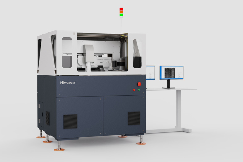
| Machine size | 1400mm*1300mm*2000mm |
| Sink size | 690mm*570mm*650mm |
| Effective scanning range | 450mm*450mm*150mm |
| Maximum scanning speed | 1000mm/s |
| Recommended image resolution | 1~4000um |
| Repeat positioning accuracy | X≤±0.003mm Y, Z≤±0.01mm |
| Water supply and drainage | Water pressure fills the water and the water pump drains water. |
| name | Specification |
| Scanning system | X-axis: linear motor module; Y-axis: screw module; Z-axis: screw module; |
| sink | 690mm*570mm*650mm |
| Ultrasonic transmitter and receiver | Bandwidth 500MHz |
| High-speed data acquisition card | Sampling frequency 1.0GHz |
| Industrial Computer | I9 processor, 32GB memory, 2T hard drive, Windows 10 64-bit operating system. |
| monitor | Two 27″ LCD monitors |
| Detection software | Hiwave Ultrasonic Nondestructive Testing Software V2.0 |
| Software Features | Functional Description |
| Manual Scan | C-scan images can be generated manually to reflect the bonding conditions of the inspected welding surfaces. The inspection results can be displayed as values such as soldering rate and defect area. The default calculation of the soldering rate is a positive peak value calculation. |
| Probe and C-scan image alignment | The probe can be moved to the position corresponding to the actual workpiece being inspected by clicking a specific pixel on the C-scan image. |
| Manual analysis | The generated C-scan images can be edited in various ways, including adding frames (to confirm the effective analysis area), measuring distance, modifying thresholds, cropping images, and performing arc compensation for arc-surface graphics. |
| Multiple scanning modes | Main scanning modes: A scanning mode, B scanning mode, C scanning mode, fast scanning, automatic scanning, area scanning and other scanning modes:
(1) A scan: The ultrasonic signal received at a certain point is imaged. The horizontal axis is time and the vertical axis is the ultrasonic signal. It can reflect the location and size of the defect. (2) B-scan: The ultrasonic signal in a certain section is displayed in a two-dimensional plane in grayscale or color. The abscissa represents the displacement direction of the scanning mechanism, and the ordinate represents the depth direction of ultrasonic propagation, reflecting the relative depth information of the defect in the sample; (3) C-scan: Scans a cross section at a certain depth. It moves in the XY two-dimensional plane and selects the signal imaging of a point at a specific depth of the A-scan, which displays the defect information of the horizontal cross section; (4) Area scanning: You can customize the detection area and scan the detection area; (5) Batch scanning: automatic inspection of one or more workpieces placed in the water tank; (6) Multi-layer C scan at one time: ≤50 layers |
| Automatic report generation | After scanning, a scanning analysis report is automatically generated, which includes: the final scanned image, various scanning parameter settings and other information. The detection results can be automatically edited and the report document can be output. |
| Probe Management | Different types of probes can be replaced or edited. |
| One-click automatic calibration | It can automatically detect the coordinate offset of the detection equipment and the energy change of the detection system, calibrate the system drift, and ensure the accuracy and stability of the detection results. |
| Stainless steel standard strength | The system comes with a stainless steel standard block that meets GBT 11259-2015 “Method for the preparation and calibration of steel comparison test blocks for ultrasonic testing”. The ultrasonic reflection intensity of the stainless steel standard block is determined to be 100 STSS (abbreviation for “Stainless Steel Standard”). The tests of all other materials are converted relative to STSS. |
| Defect detection capabilities | Areas with welding defects, bonding defects, package delamination, die bonding voids, etc. and good areas.
The defect size and area can be automatically counted and calculated. We can also provide paid customized development services according to customer requirements. |
| Sound speed detection | The speed at which sound travels through the material being measured. |
Semiconductor devices and packaging
Plastic packaged IC , flip chip FipChip, chip scale package CSP, BGA (metal, plastic package), molded underfill (MUF), hybrid multi-chip module (MCM), stacked chip imaging (SDI), discrete devices, 1GBT and other high-power semiconductor devices, etc.
Wafer bonding wafer, MEMS, LED, BSI Sensors, TSV, etc.
Other microelectronic multilayer ceramic capacitors (MLCC), ceramic packaging tubes and shells, semiconductor electronic refrigerators, aerospace components, etc.
Material testing: diamond composite sheets, ceramics, glass, metals, welded parts, etc.
Plastic package IC
PBGA
Flip chip
High power rectifier device thyristor
Ceramic Capacitors
Package
Electrostatic Ceramic Tray
Water cooling plate/heat sink
Hiwave specializes in providing ultrasonic scanning microscopes (USM) for precise non-destructive testing in semiconductors and electronics.