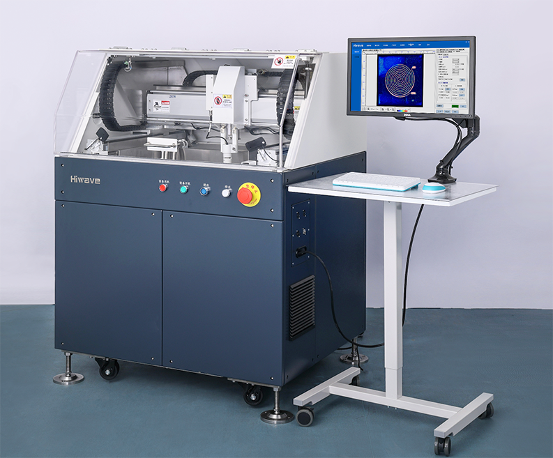
Hiwave Scanning Acoustic Microscope for Wafer Bonding
views:1,400
author:admin
source:Hiwave
time:2024-12-27
catogory:Industry News
The Importance of Wafers
Wafers are the basis for the manufacture of integrated circuits (ICs), transistors, LEDs……
Principles of water immersion SAM:
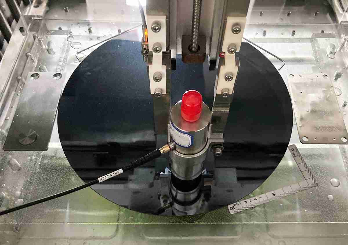
The ultrasonic C-scan inspection system uses high-frequency sound waves to examine internal defects in materials. Its working principle can be simplified into the following steps:
1.Emission of Ultrasonic Waves:
The transducer (probe) in the system emits high-frequency sound waves into the material to be inspected, such as a weld.
2.Reception of Reflected Signals:
When these sound waves encounter internal defects (like cracks or porosity) or interfaces between different materials, they reflect back. The probe receives these reflected waves and converts them into electrical signals.
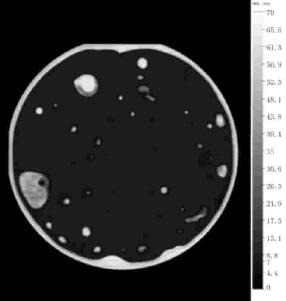
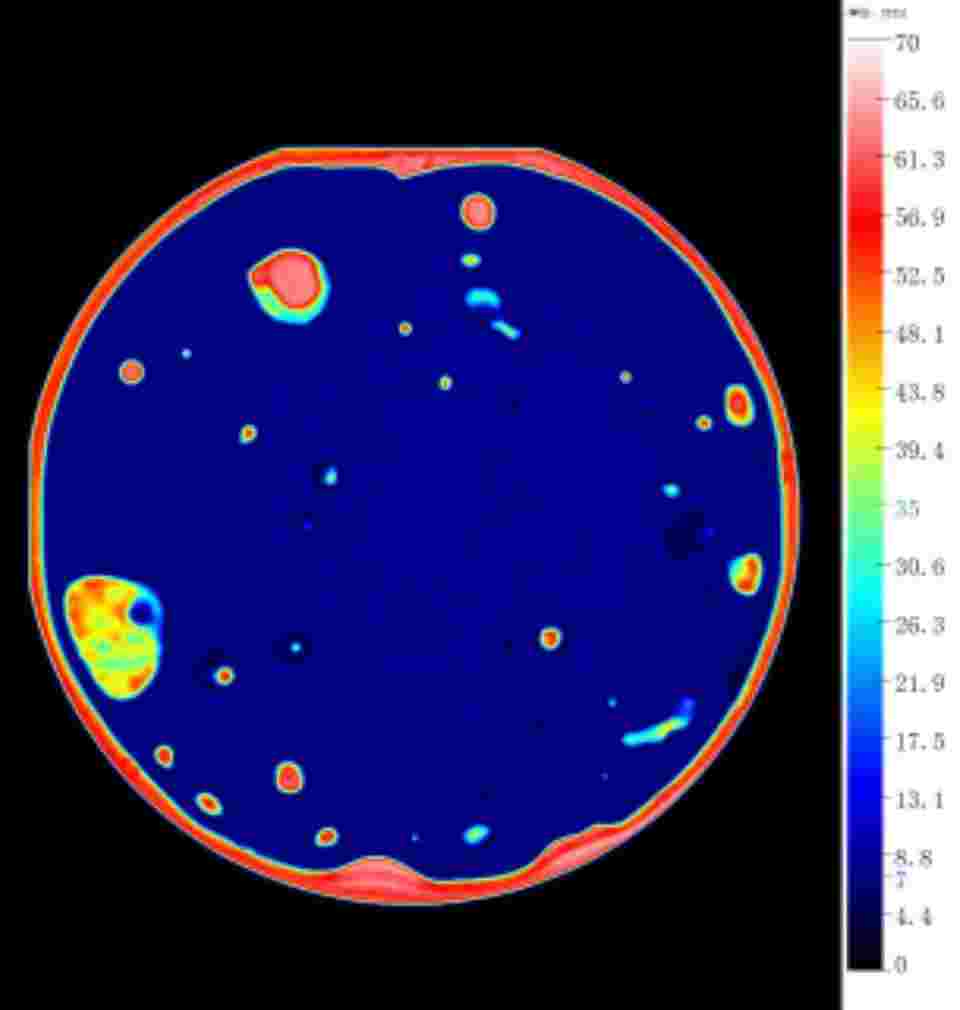
3.Image Generation:
The received signals are processed to generate a two dimensional image (C-scan) that shows the location and relative size of defects within the material.
4.Defect Analysis:
By analyzing the intensity and characteristics of the reflected signals in the image, the quality of the weld can be assessed, determining the type, size, and position of any defects.
Bonding defects inside wafers can be clearly seen in the inspection images from the Hiwave S600 equipment. These high-resolution images not only show the location of the defects, but also provide key information on the type, size and distribution of the defects, providing insight into the quality of the wafer and optimizing production.
As a leading ultrasonic scanning microscope company in China, Shanghai Hiwave has developed ultrasonic scanning microscopes that have been recognized by many companies, such as Huawei, BYD, Siemens, Schneider, Tata, and Saudi Aramco.