5-Step Guide to Improve Semiconductor Defect Detection Accuracy
views:902
author:admin
source:Hiwave
time:2025-02-07
catogory:Industry News
In the semiconductor industry, ensuring the highest quality and reliability of components is paramount. Defect detection plays a crucial role in maintaining these st……
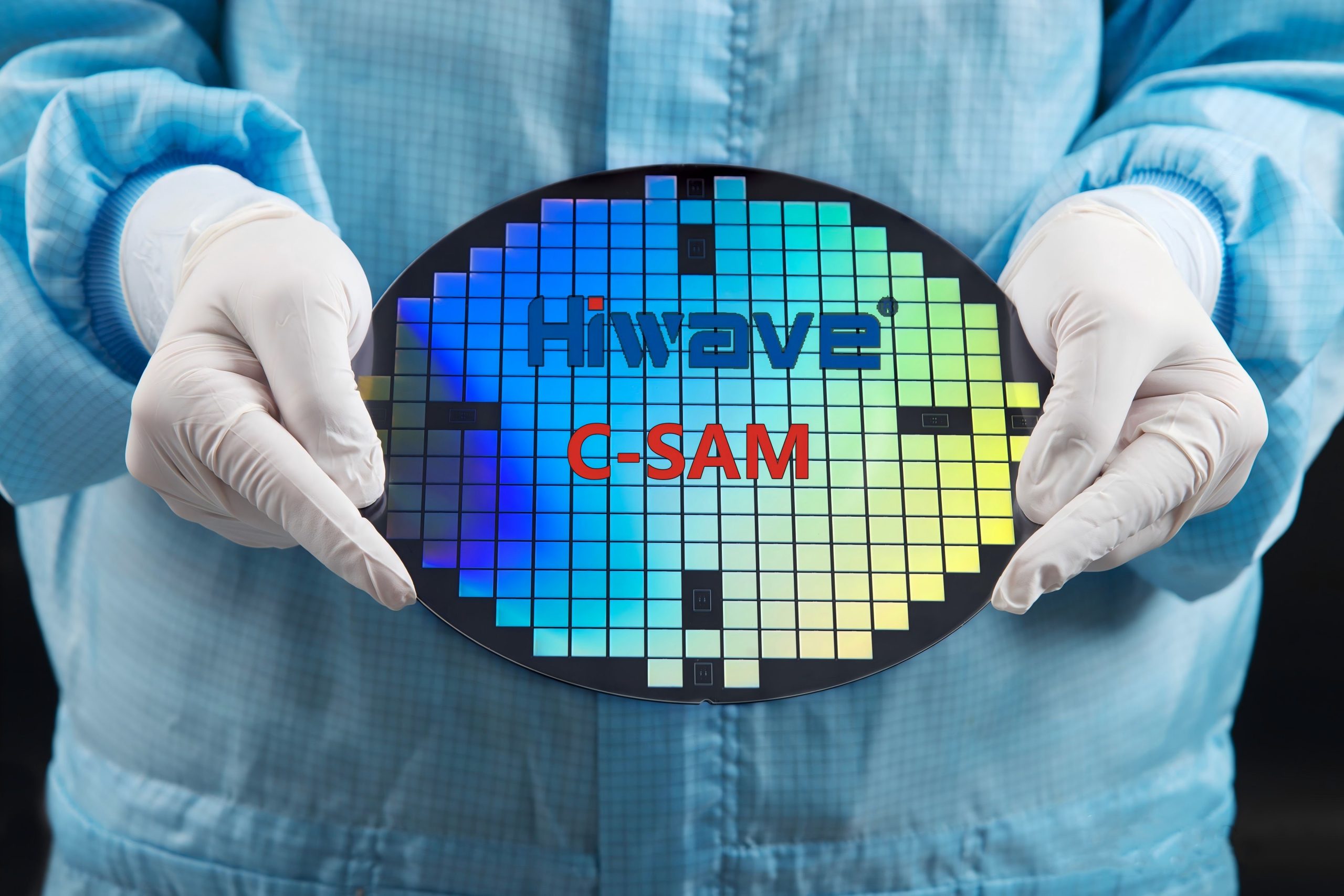
In the semiconductor industry, ensuring the highest quality and reliability of components is paramount. Defect detection plays a crucial role in maintaining these standards, and advancements in technology have made it possible to achieve unprecedented levels of accuracy. As a leading manufacturer of ultrasonic scanning microscopes (SAM), Hiwave is dedicated to defect detection. Here’s a 5-step guide to improving semiconductor defect detection accuracy using water-immersion ultrasonic scanning microscopy technology.
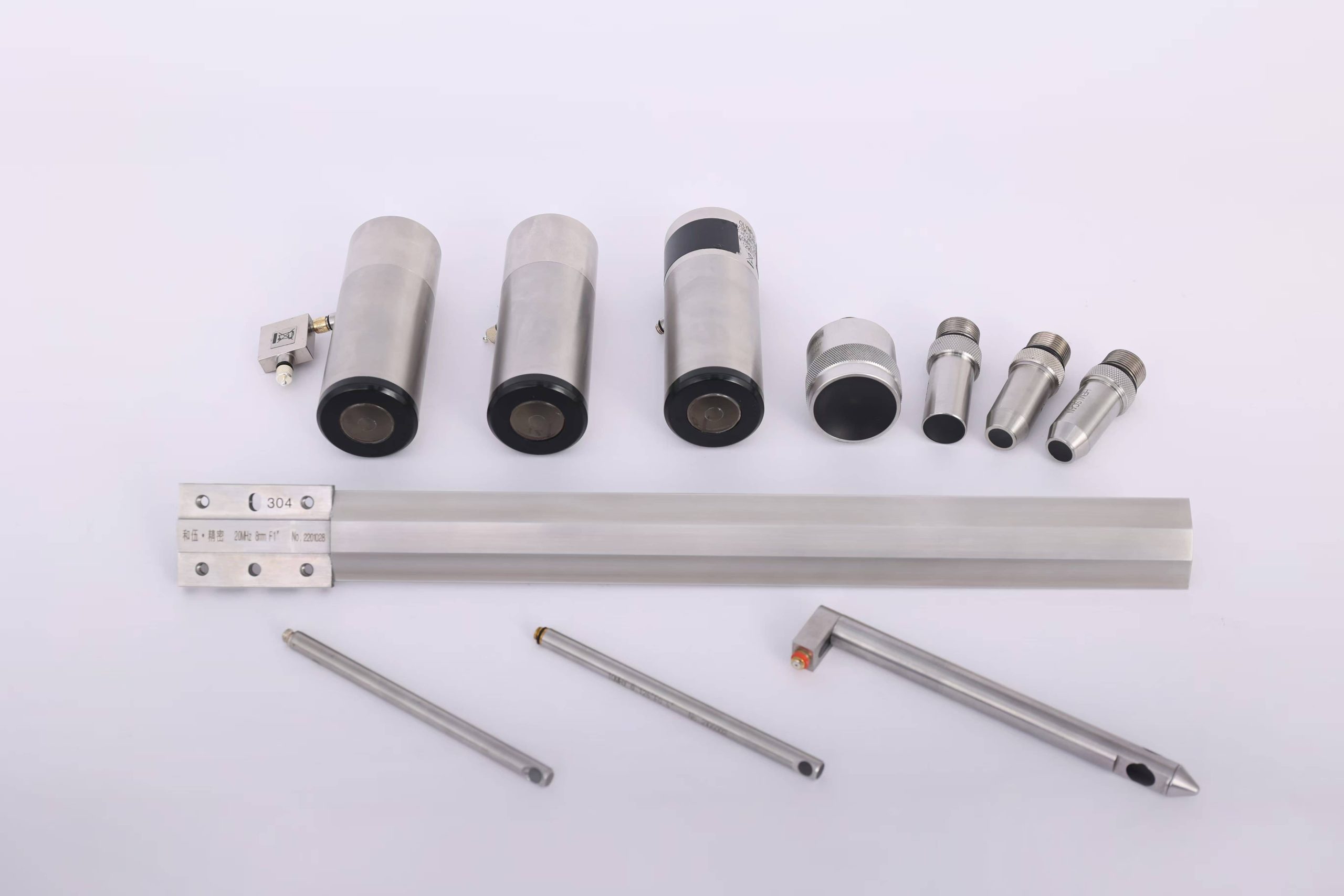
Step 1: Optimize Probe Ultrasonic Frequency Selection
The frequency of the probe used in scanning microscopy significantly impacts defect detection accuracy. Higher frequencies provide better resolution for detecting smaller defects, while lower frequencies penetrate deeper into the material. To optimize results:
Analyze Material Properties: Choose the appropriate frequency based on the material thickness and type.
Balance Resolution and Penetration: For surface-level defects, use higher frequencies (e.g., 100 MHz or above). For deeper defects, opt for lower frequencies (e.g., 10-50 MHz).
Utilize Multi-Frequency Scanning: Employ advanced SAM systems that support multiple frequencies for comprehensive defect analysis.
Step 2: Enhance Signal Processing Algorithms
Accurate defect detection relies on the ability to interpret ultrasonic signals effectively. Modern SAM systems are equipped with advanced signal processing algorithms that can distinguish between noise and actual defects. To improve accuracy:
Implement AI-Driven Analysis: Use machine learning algorithms to identify patterns and anomalies in the ultrasonic data.
Reduce Noise Interference: Apply filtering techniques to eliminate background noise and enhance signal clarity.
Automate Defect Classification: Integrate software solutions that automatically classify defects based on size, shape, and location.
Step 3: Regularly Calibrate Equipment
Regular calibration of your ultrasonic scanning microscope is essential to maintain accuracy and consistency. Even minor deviations can lead to missed defects. Follow these best practices:
Schedule Routine Calibration: Perform calibration before critical inspections or at regular intervals.
Use Certified Reference Standards: Ensure calibration is done using industry-standard reference materials.
Monitor System Performance: Track key performance metrics to identify and address any drift in accuracy.
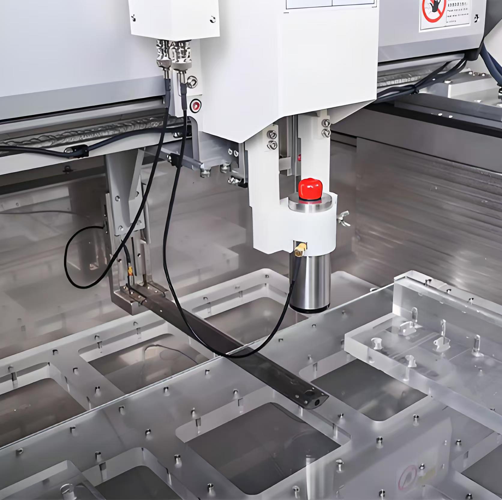
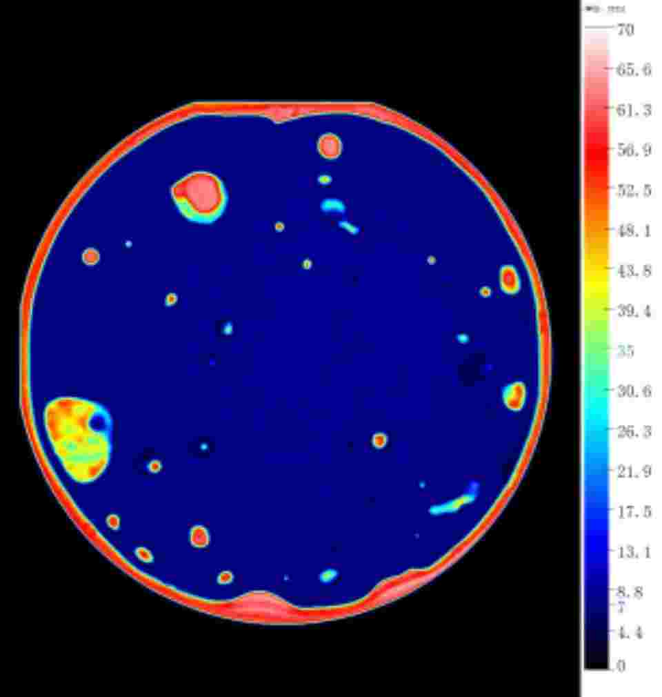
Step 4: Implement Advanced Imaging Techniques
Traditional ultrasonic imaging may not always provide the clarity needed to detect subtle defects. Advanced imaging techniques can significantly enhance defect visibility:
Tomographic Reconstruction: Combine multiple scans to create cross-sectional images, revealing hidden defects.
Real-Time Imaging: Leverage real-time scanning capabilities to monitor defects as they occur during production.
Step 5: Effectively Train Your Team
Even the most advanced equipment cannot deliver optimal results without skilled operators. Investing in training ensures your team can fully utilize the capabilities of your SAM system:
Provide Hands-On Training: Equip your team with practical experience in operating the equipment and interpreting results.
Stay Updated on Industry Trends: Regularly update your team on the latest advancements in ultrasonic scanning technology.
Encourage Collaboration: Foster a culture of knowledge sharing to continuously improve defect detection processes.