Failure Analysis of Scanning Acoustic Microscope for IC
views:5,141
author:Hiwave
source:Hiwave
time:2025-02-21
catogory:Industry News
With the continuous increase in complexity and integration of integrated circuits, chip manufacturing processes require higher sensitivity and precision for defect d……
With the continuous increase in complexity and integration of integrated circuits, chip manufacturing processes require higher sensitivity and precision for defect detection. Although traditional optical microscopes and X-ray techniques are widely used in IC inspection, they have certain limitations in identifying critical defects such as internal interface delamination, cracks, and voids.
Scanning acoustic microscopy, as a non-destructive and high-resolution inspection method, has demonstrated unique advantages in the field of IC packaging and testing in recent years.
Working Principle of Scanning Acoustic Microscopy
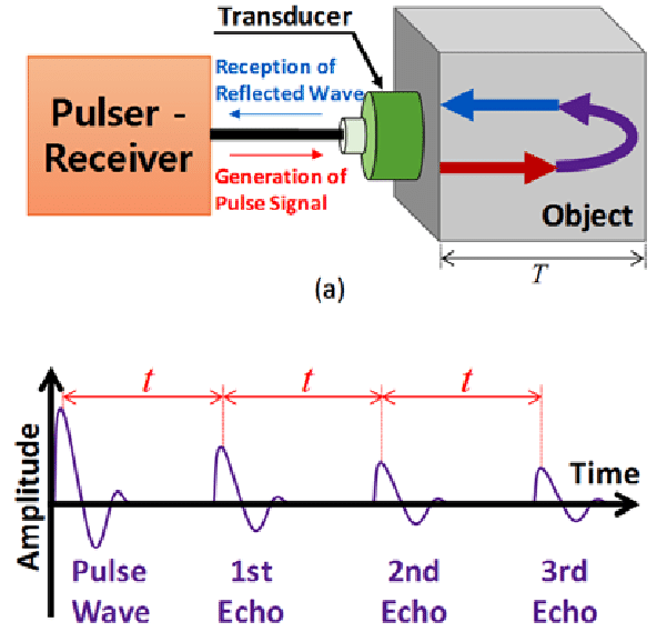
Scanning acoustic microscopy operates based on the reflection and transmission characteristics of high-frequency ultrasound waves (typically ranging from 10 MHz to 200 MHz). The core principle involves using a piezoelectric transducer to emit ultrasonic waves, which penetrate the sample being tested. The transducer then receives the reflected or transmitted echo signals, which are processed to generate high-resolution two-dimensional or three-dimensional images.
Due to differences in acoustic impedance between different materials or interfaces, ultrasonic waves undergo significant reflection or scattering at defect sites such as cracks and voids. These reflections or scatterings result in noticeable differences in the image, often represented by variations in color or intensity.
Application in IC Defect Detection
Encapsulation Interface Delamination Detection
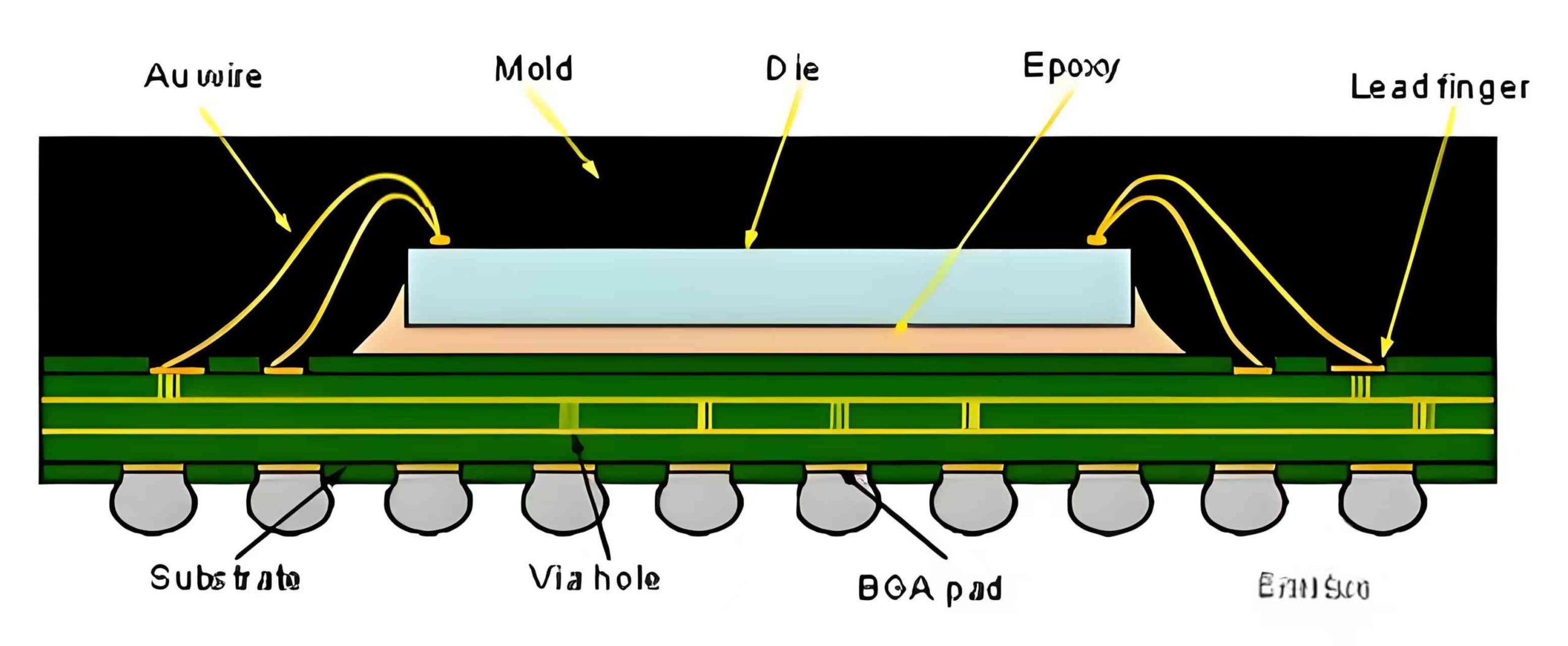
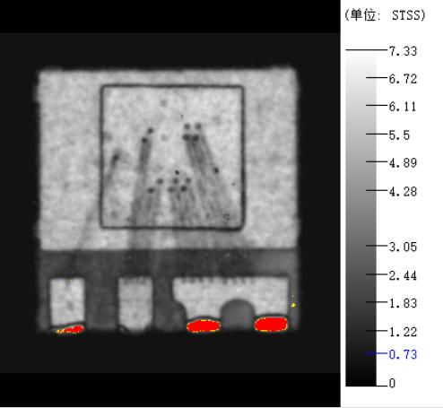
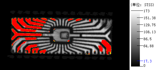
During the IC encapsulation process, interfaces between the chip and substrate, or between the molding compound and solder balls, can suffer delamination due to thermal stress or poor manufacturing processes. Scanning Acoustic Microscopy (SAM) can clearly identify these minute separations (with resolution down to the micrometer level) and generate two-dimensional distribution maps of delamination areas through C-Scan mode, helping to locate defect positions.
Solder Joint Void and Crack Detection
In Ball Grid Array (BGA) or Flip-Chip packaging, the quality of solder joints directly affects circuit reliability. SAM can detect micro-bubbles, voids, or micro-cracks within the solder joints by analyzing the propagation paths of ultrasonic waves. This helps avoid early failures caused by poor soldering.
Wafer-Level Packaging (WLP) Quality Control
In wafer-level packaging, SAM can be used to inspect the fill integrity of Through-Silicon Vias (TSVs), the bonding status of Redistribution Layers (RDL), and defects in temporary bonding/debonding processes. This significantly improves yield rates.
Failure Analysis and Reliability Testing
After IC aging tests (such as temperature cycling and humidity testing), SAM can non-destructively evaluate whether internal materials have developed micro-defects due to accumulated stress. This provides critical data for failure mechanism analysis.
Scanning acoustic microscopy, with its unique acoustic imaging capabilities, has become an indispensable tool in IC defect detection. As semiconductor packaging technology evolves towards high-density and three-dimensional integration, the role of SAM in process optimization, quality control, and failure analysis will become even more prominent. In the future, by integrating with other detection technologies such as infrared thermography and X-ray CT, SAM is expected to provide more comprehensive defect management solutions for IC manufacturing.
If you want to get more information,please contact
Email:service@ihiwave.com
Website:www.ehiwave.com