Application of Scanning Acoustic Microscopy in Defect Inspection of Underfill on PCBA
views:475
author:admin
source:Hiwave
time:2025-12-05
catogory:Industry News
Scanning Acoustic Microscopy (SAM) is a high-precision, non-destructive testing technique that utilizes high-frequency ultrasound to inspect the internal structure o……
Scanning Acoustic Microscopy (SAM) is a high-precision, non-destructive testing technique that utilizes high-frequency ultrasound to inspect the internal structure of materials. It is particularly well-suited for detecting microscopic defects—such as interfacial delamination, voids, and cracks—between encapsulants (e.g., underfill) and Printed Circuit Board Assemblies (PCBAs).
Ultrasonic Wave Propagation Characteristics
When ultrasonic waves propagate through a material, they undergo reflection, refraction, or scattering upon encountering interfaces with different densities or elastic properties (e.g., between underfill and a silicon die or PCB substrate). By analyzing the amplitude, phase, and time delay of the reflected signals, SAM reconstructs high-resolution images of the internal structure.
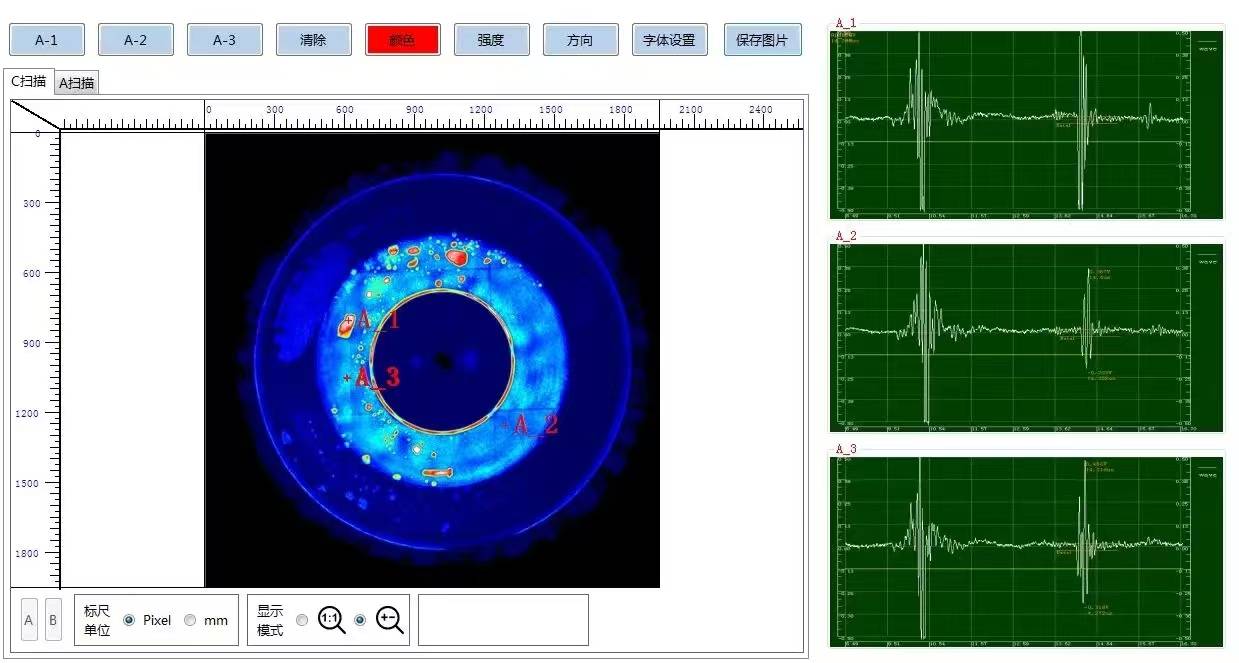
Detection Modes
A-Scan (Amplitude Scan): Displays the amplitude of reflected signals versus time, used to determine defect depth.
B-Scan (B-Scan): Generates a two-dimensional cross-sectional image, revealing internal layer structures.
C-Scan (C-Scan): Produces a three-dimensional top-down image through point-by-point scanning, providing an intuitive visualization of defect distribution.
Key Advantages for PCBA + Underfill Inspection
Non-Destructive Testing:
No sample destruction is required, making it ideal for in-line sampling in mass production or failure analysis.
High Resolution:
Capable of detecting micron-scale defects (e.g., voids ≥50 μm in diameter), significantly surpassing the resolution of X-ray imaging (typically ≥200 μm).
Strong Penetration Capability:
Ultrasound can penetrate opaque materials such as underfill and molding compounds to inspect internal interfaces.
Broad Material Compatibility:
Suitable for a wide range of substrates—including metals, ceramics, plastics, and composites—and especially effective for multi-layer structures (e.g., chip–underfill–PCB).
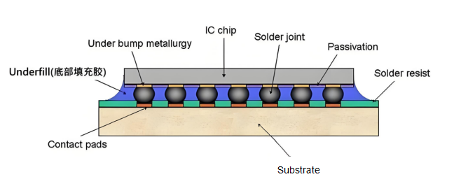
Typical Inspection Applications
Underfill Fill Quality Assessment
Voids: Unfilled cavities within the underfill that may lead to thermal stress concentration or mechanical failure.
Delamination: Separation at the interface between underfill and the chip or PCB substrate.
Cracks: Micro-cracks within the underfill or at its interfaces.
Solder Joint Inspection
Detects voids or cold solder joints beneath Ball Grid Array (BGA) packages.
Package Integrity Verification
Confirms the adhesion quality between molding compound and the die or lead frame.