Application of Water Immersion Acoustic Microscope in Chip Packaging
views:688
author:Hiwave
source:Hiwave
time:2025-02-24
catogory:Industry News
Chip packaging (IC Packaging) is a crucial step in semiconductor manufacturing. Its purpose is to protect the bare dies (cut from wafers) and provide electrical conn……
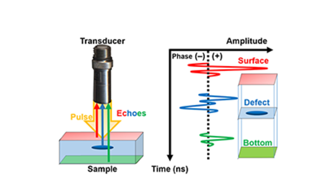
Chip packaging (IC Packaging) is a crucial step in semiconductor manufacturing. Its purpose is to protect the bare dies (cut from wafers) and provide electrical connections and physical support to external circuits. Packaging not only affects chip performance (such as heat dissipation and signal transmission) but also directly determines its reliability and cost. The water immersion scanning acoustic microscope is an essential tool for inspecting chip packaging. Its detection principle is as follows:
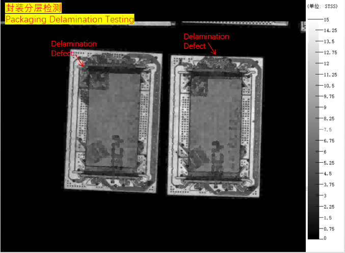
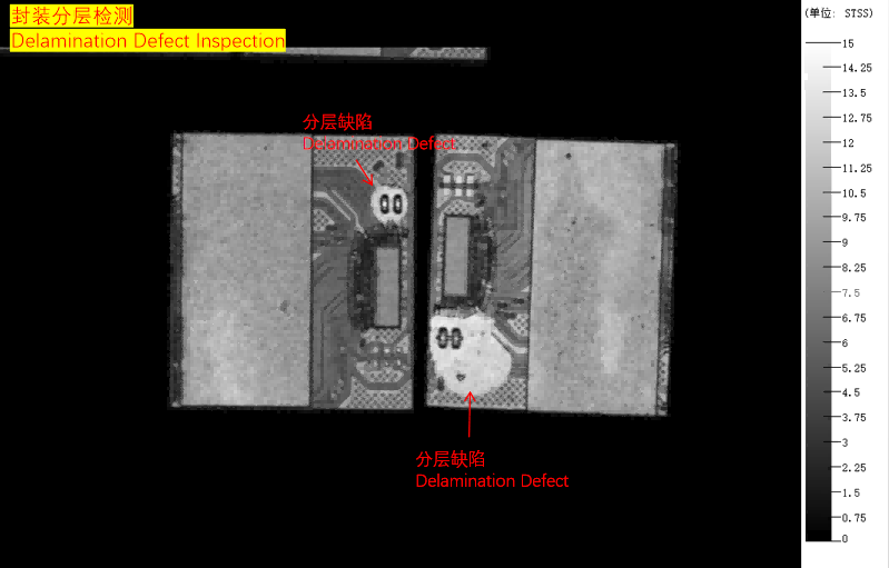
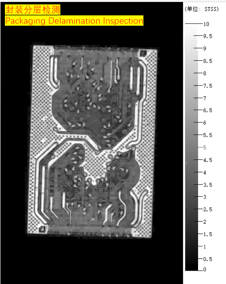
A Water Immersion Scanning Acoustic Microscope (SAM) uses high-frequency ultrasonic waves coupled with water. By leveraging the reflection/refraction and phase difference characteristics of sound waves, it achieves non-destructive, high-resolution imaging of defects (such as voids, delamination, cracks) in chip packaging. It can penetrate complex structures (like BGA, 3D IC) and, combined with AI algorithms, quickly locates micron-level defects and evaluates material and interface reliability. This provides critical support for optimizing packaging processes and improving yield rates.
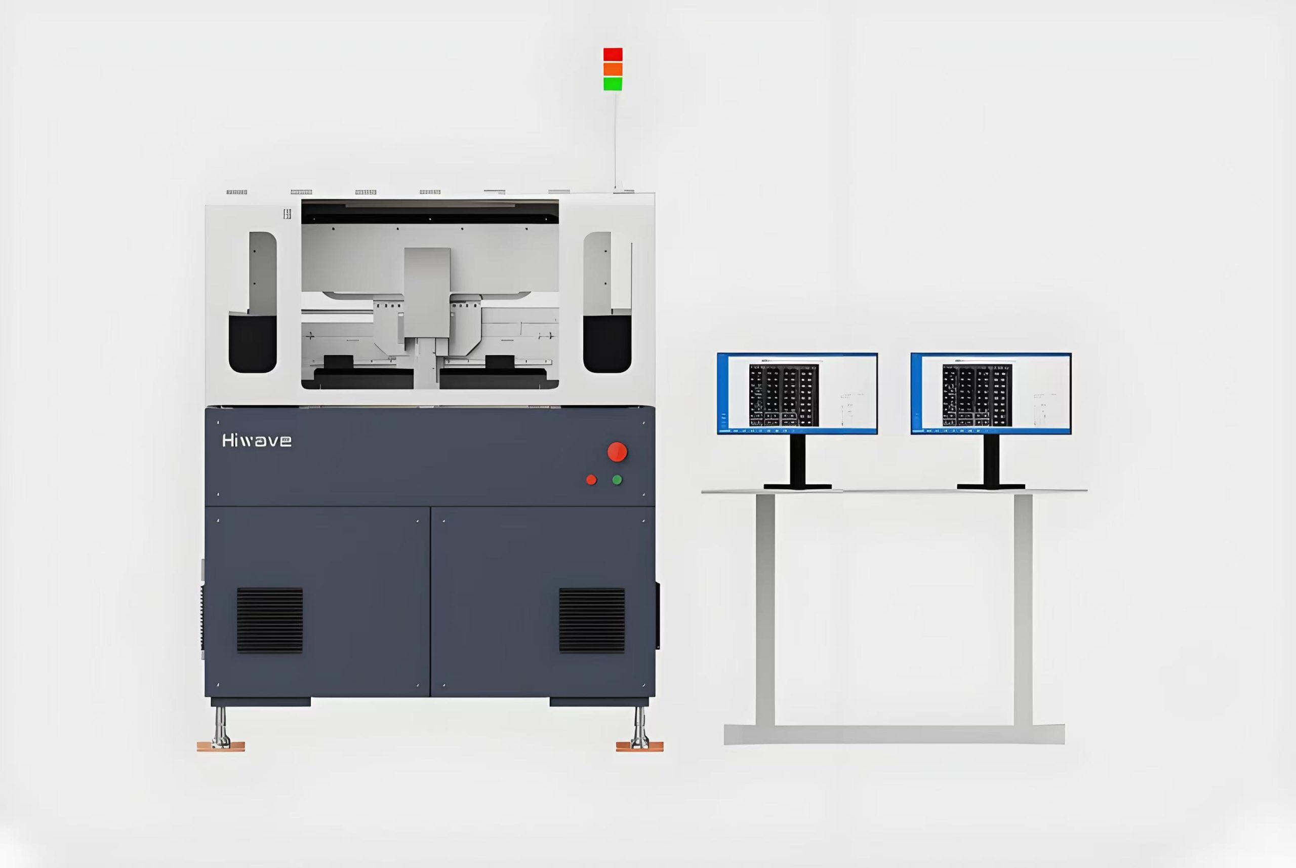
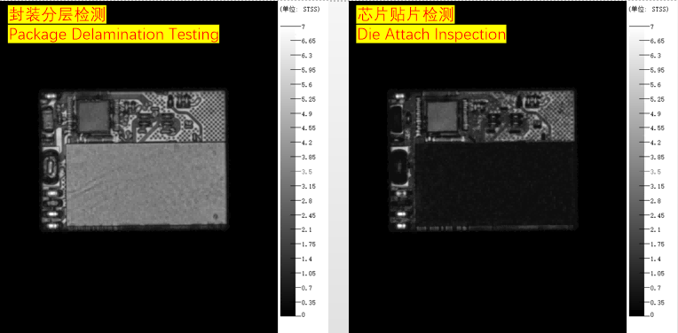
Below is a solution for detecting plastic-encapsulated chips using the Hiwave S600 device.
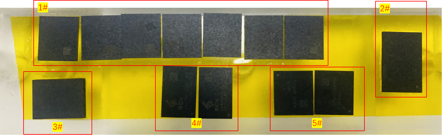
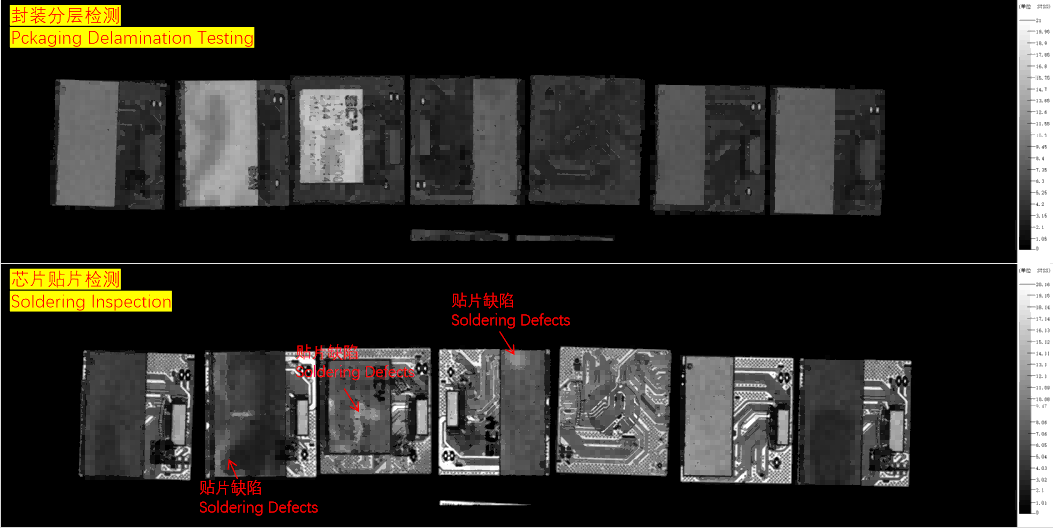
Due to the rough surface of the samples, a 50 MHz – 0.5-inch probe is used for detection. The following are the resulting images.