Applications of Scanning Acoustic Microscopy in Chip Packaging: TO/BGA/SOT/SOP
views:1,029
author:Hiwave
source:Hiwave
time:2025-03-28
catogory:Industry News
As a core representative of the third-generation non-destructive testing technology, ultrasonic scanning microscopy (SAM) is redefining industry standards for semico……
As a core representative of the third-generation non-destructive testing technology, ultrasonic scanning microscopy (SAM) is redefining industry standards for semiconductor packaging inspection. In today’s era of rapid iteration in miniaturization technology, different packaging types such as TO, BGA, SOT, and SOP present differentiated demands for inspection techniques. With its unique penetration imaging capability, SAM demonstrates irreplaceable technical advantages in micrometer-level defect detection.
Different Types of Packaging
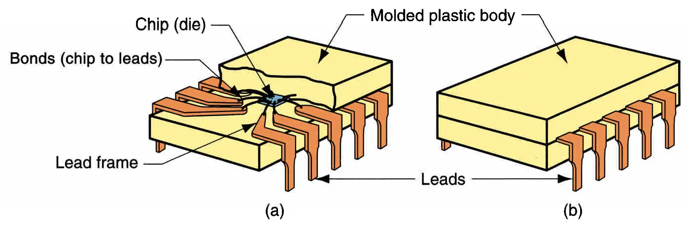
TO (Transistor Outline) packaging is commonly used for discrete components such as transistors or diodes. It has a relatively simple structure with fewer pins. BGA (Ball Grid Array) packaging features pins arranged in the form of solder balls at the bottom, and it is commonly used for high-performance chips with high integration, making inspection more challenging. SOT (Small Outline Transistor) packaging is smaller than TO and suitable for surface mounting, often found in small-signal devices.
Inspection Cases
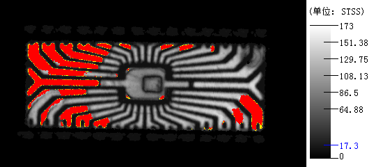
TO Series Packaging: Detect delamination defects at the copper ribbon bonding interface to prevent power device failures caused by thermal stress.
SOT Packaging: Identify micro-cracks in the dielectric material within 3D heterogeneous integration to prevent signal transmission interruptions.
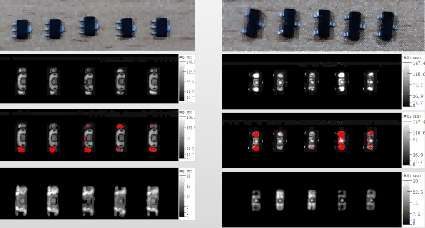
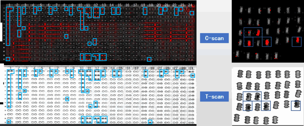
SOP Series Packaging Chips