Scanning Acoustic Microscope in Chip Package and Assembly Testing
views:1,139
author:Hiwave
source:Hiwave
time:2025-04-10
catogory:Industry News
With the rapid development of the semiconductor industry, the requirements for quality control in chip packaging and assembly processes are becoming increasingly str……
With the rapid development of the semiconductor industry, the requirements for quality control in chip packaging and assembly processes are becoming increasingly stringent. The Scanning Acoustic Microscope (SAM), as a non-destructive testing tool, plays a crucial role in this field.
Introduction to Scanning Acoustic Microscope
The Scanning Acoustic Microscope uses ultrasonic waves to image the internal structure of materials, enabling clear visualization of subtle defects such as cracks, delamination, and voids within samples. Its working principle is based on the reflection characteristics of ultrasonic waves at interfaces between different media. By analyzing these reflected signals, SAM achieves high-resolution imaging of the material’s internal structure.
Applications in Chip Packaging
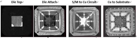
Layered Inspection:
Chip to Adhesive Layer: During the chip packaging process, it is essential to ensure that the bonding between the chip and the adhesive layer is tight and free of defects. Using SAM, it is possible to effectively detect whether there are bubbles or incomplete bonding between these two layers.
Adhesive Layer to Material Layer: The bonding between the adhesive layer and subsequent material layers is equally critical. Any discontinuity or delamination will affect the stability of the entire package structure. SAM can precisely identify problematic areas, providing a basis for process improvements.
Material Layer to Copper Wire Layer: In modern chip packaging, copper wires are often used to connect different components. SAM can help inspect the contact between the copper wires and surrounding materials, ensuring reliable electrical connections.
Copper to Substrate Layer: Finally, the copper wires need to be securely fixed to the substrate. SAM can be used in this step to verify the welding quality between the copper wires and the substrate, preventing functional failures caused by poor soldering.
Defect Detection: In addition to the layered inspection mentioned above, SAM can also detect other types of internal defects, such as cracks and voids, thereby comprehensively evaluating the quality of the package.
Package Integrity Assessment: SAM is not limited to localized inspections but can also evaluate the overall integrity of the package structure, ensuring no damage or abnormalities have occurred during the packaging process.
Material Interface Analysis: SAM can also perform detailed analysis of the interfaces between packaging materials, which is of great significance for studying the effectiveness of new materials and optimizing packaging processes.
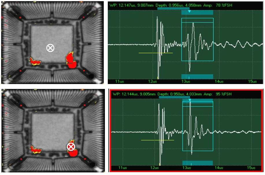
Assembly Testing
After the chip assembly is completed, a series of rigorous tests are typically required to ensure that the connections between components are secure and meet the design requirements for electrical performance. SAM can check the quality of solder joints in a non-contact manner, identifying potential issues such as cold solder joints or short circuits. This is crucial for improving yield rates and product quality.
In summary, the Scanning Acoustic Microscope not only provides effective quality control measures for chip packaging and assembly but also, with its non-destructive testing capabilities, has become an indispensable part of modern semiconductor manufacturing. Particularly in layered inspections, SAM demonstrates its unique advantages, offering strong support to ensure tight bonding at every level. As technology advances, the application scope of SAM will continue to expand, making greater contributions to the development of the entire industry.