Scanning Acoustic Microscopy (SAM) for Detecting Delamination in Chip Welds
views:1,435
author:admin
source:Hiwave
time:2024-12-23
catogory:Industry News
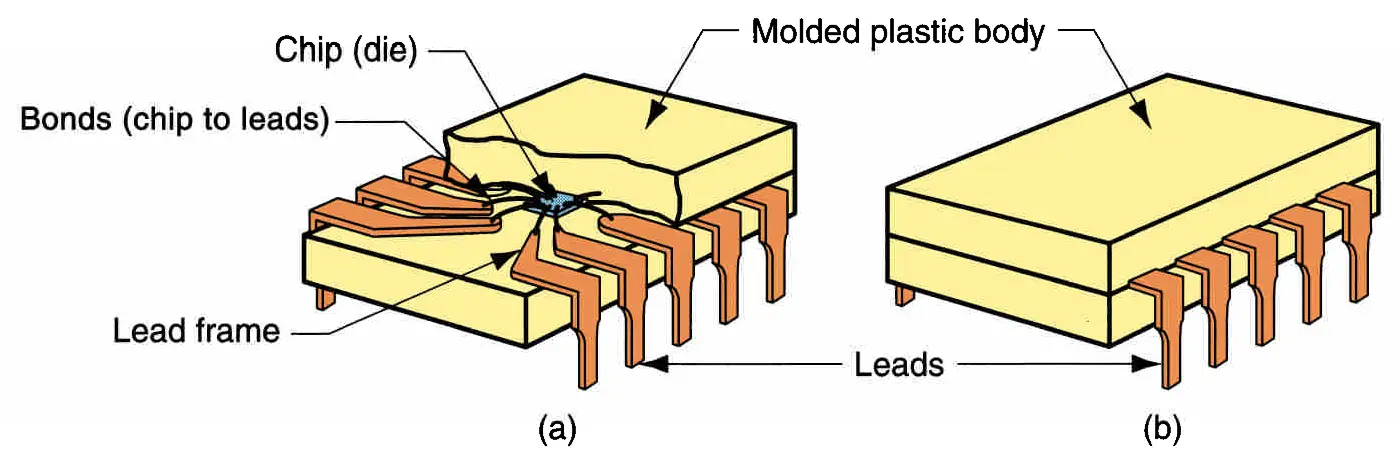
The Importance and Structure of Plastic Encapsulated Chips
In semiconductor packaging, welding defects during chi……
The Importance and Structure of Plastic Encapsulated Chips
In semiconductor packaging, welding defects during chip mounting have persistently challenged package quality and yield. As a primary procedure in packaging high-power electronics, chip attachment using soft solder or silver paste can introduce voids and delamination, significantly impacting device performance and longevity. Thus, assessing weld quality is essential for ensuring device reliability.
Inspection Methods for Plastic Encapsulated Chips
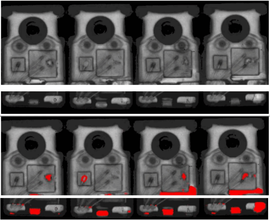
Radiographic methods for inspecting plastic encapsulated chips have shortcomings in image resolution, efficiency, and the detection and analysis of delamination defects.
Ultrasonic Scanning Microscopy (USM), however, excels in these areas by using high-frequency ultrasound, fast data acquisition, and precise movement systems to provide accurate, efficient online inspections. Its software can instantly show detailed cross-sectional images of the chip’s internal structure during scanning.
The principle of scanning acoustic microscope
Ultrasonic Scanning Microscopy (USM) utilizes the propagation characteristics of ultrasonic waves, transmitting signals into the material and capturing the echoes that return after interacting with internal structures. The speed and reflection behavior of ultrasonic waves vary according to the physical attributes of the media encountered, including density and elastic modulus.
Upon encountering interfaces between different materials or internal defects, ultrasonic waves exhibit behaviors such as reflection, refraction, or scattering. Analysis of the reflected wave characteristics allows USM to generate high-resolution imagery, exposing the material’s internal microstructure and any latent defects, which in turn influences the accuracy of the scanning process.