How to test packaging chips with scanning acoustic microscope
views:976
author:admin
source:Hiwave
time:2025-01-09
catogory:Industry News
What is a Scanning Acoustic Microscope (SAM)?
A Scanning Aco……
What is a Scanning Acoustic Microscope (SAM)?
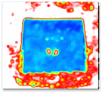
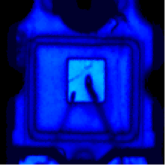
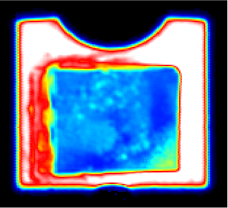
A Scanning Acoustic Microscope (SAM) is a non-destructive testing tool that utilizes ultrasound waves to inspect the internal structure and defects of materials. It finds extensive applications in industries such as electronics, semiconductor manufacturing, and materials science, particularly for evaluating packaged chips, assessing the quality of solder joints, and performing non-destructive testing on composite materials.
Common Defects in Semiconductor Packaging
Principles of Ultrasonic Inspection
Ultrasonic Wave Generation and Emission
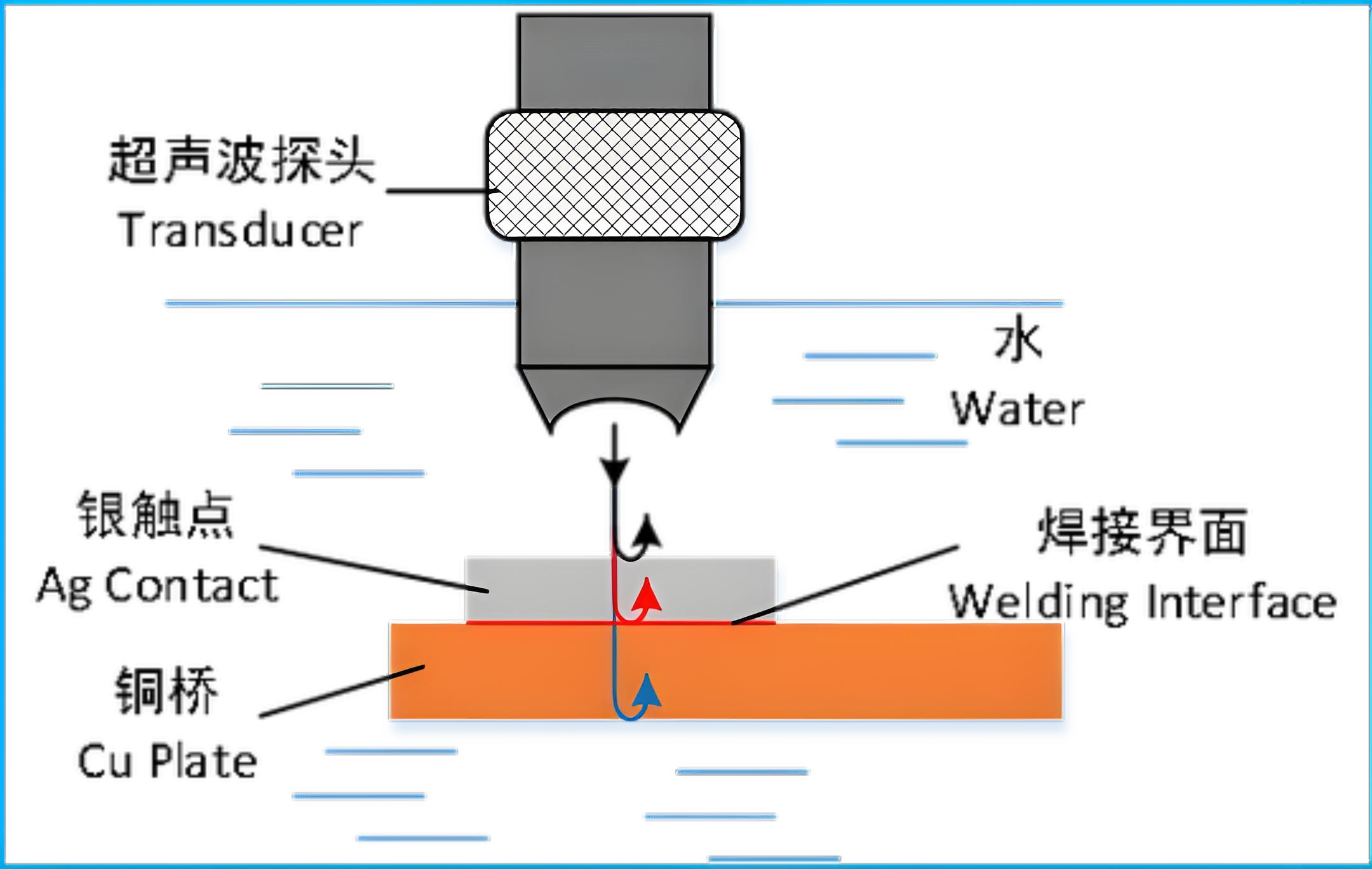
Scanning Acoustic Microscopy (SAM) uses piezoelectric crystals or other types of transducers to generate high-frequency ultrasonic pulses. These ultrasonic waves have a specific frequency range, typically from several megahertz to hundreds of megahertz, depending on the required detection resolution and penetration depth.
Propagation and Interaction of Ultrasonic Waves
When ultrasonic waves enter a sample, they travel through different material layers and interact with interfaces between materials by reflecting, refracting, or transmitting.
If there are internal defects in the material (such as voids, cracks, delaminations), the ultrasonic waves will produce abnormal reflection signals at these defect sites because the acoustic impedance of the defect areas differs from that of the surrounding material.
Signal Acquisition and Processing
The reflected ultrasonic waves are captured by the same or another receiver and converted into electrical signals. This process involves transforming mechanical vibrations into measurable electronic signals.
The strength of the received signal and the time delay provide information about the internal structure of the sample, such as interface locations, thickness, and any existing defect characteristics.
Image Reconstruction
By moving the sample stage or the transducer, scanning can be performed across the entire surface of the sample, collecting data from multiple points.
All collected data are used to construct two-dimensional or three-dimensional ultrasonic images that reveal various layers and structural features within the sample.
These images can display the distribution of internal defects, such as the position, size, and shape of voids; the direction and length of cracks; and the quality of bonding between different material layers.
Leading Scanning Acoustic Microscope supplier of China