How to test transistor outline(TO) with scanning acoustic microscope
views:569
author:admin
source:Hiwave
time:2025-01-10
catogory:Industry News
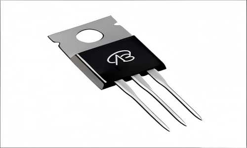
What is TO Chip Packaging
TO series chip packaging, which stands for Transistor Outline, is a category of standar……
What is TO Chip Packaging
TO series chip packaging, which stands for Transistor Outline, is a category of standard packaging formats used for semiconductor devices. This type of packaging is primarily utilized for discrete components such as power transistors, diodes, thyristors, and more, and is well-known for its standardized physical dimensions and pin configurations. TO packages can be made from metal or plastic, featuring various numbers of pins and mounting methods (such as through-hole or surface mount), with some designs incorporating heat sinks to enhance thermal performance.
What is Scanning Acoustic Microscope (SAM)
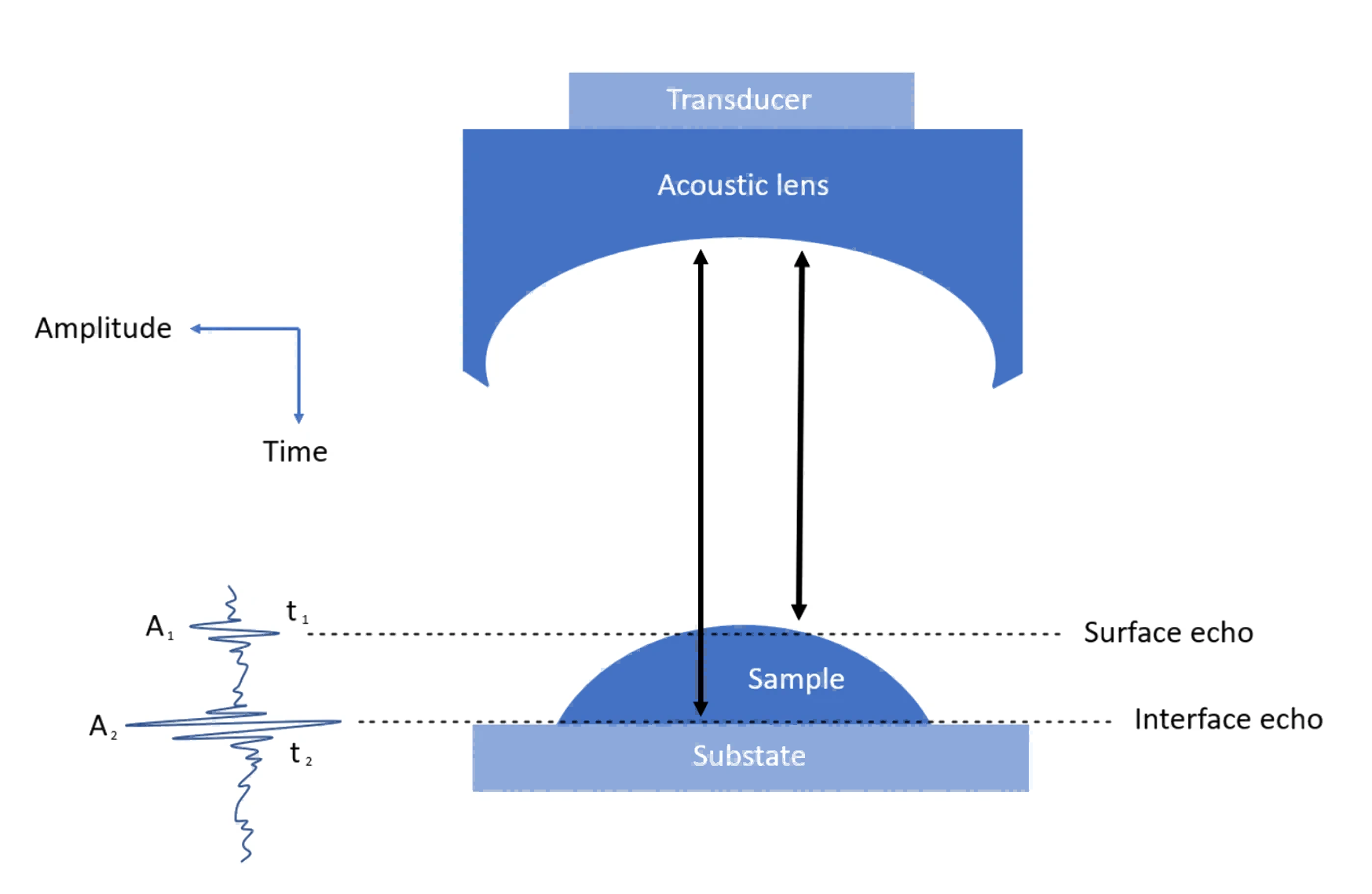
A Scanning Acoustic Microscope (SAM) is an instrument that employs high-frequency ultrasound waves for the non-destructive testing and imaging of samples. By analyzing the information from the reflection, refraction, or scattering of ultrasound waves at different material interfaces, SAM can provide detailed images of a sample’s internal structure and characteristics. This technology finds extensive applications in fields such as materials science, electronics industry, biology, etc., particularly in evaluating material defects, delamination, cracks, bond quality, and thickness measurements.
Working Principle of Scanning Acoustic Microscope
Ultrasonic Wave Emission:The Scanning Acoustic Microscope (SAM) utilizes a probe to emit high-frequency ultrasonic pulses, typically ranging from several megahertz to hundreds of megahertz. These pulses penetrate the surface of the sample and travel into its interior.
Interaction:When ultrasonic waves encounter interfaces between materials of different densities or elasticities, phenomena such as reflection, refraction, or scattering occur. Different materials exhibit varying absorption and reflection characteristics of ultrasonic waves, which depend on their acoustic impedance.
Signal Reception and Processing:
The probe, responsible for emitting ultrasonic waves, also receives the signals reflected back from the internal structures of the sample. The system then converts these received signals into electrical signals, which are processed through specialized computer software.
Image Generation:
The processed data is used to construct two-dimensional or three-dimensional images of the sample’s internal structure. In these images, grayscale or color variations represent changes in the intensity of the reflected ultrasonic waves, thereby reflecting the differences in the physical properties within the material.
Application of SAM Technology in TO Package Defect Detection
Scanning Acoustic Microscope (SAM) technology plays a crucial role in the detection of defects in TO packages. By emitting high-frequency ultrasonic waves and analyzing the signals reflected back from the internal structures of the sample, SAM can non-destructively reveal detailed information about the interior of TO series chip packages. Using SAM, engineers can accurately identify hidden defects such as voids, cracks, and delamination, which are often undetectable by traditional optical inspection methods.
SAM not only provides high-resolution internal images but also allows for multi-angle, multi-layer inspections without compromising the integrity of the sample. This capability is essential for ensuring the reliability and performance of TO-packaged products. Furthermore, SAM technology aids in optimizing manufacturing processes by detecting potential issues early, thereby reducing defect rates and providing data support for design improvements, significantly enhancing the overall quality of electronic devices.
Founded in 2012, Shanghai Hiwave Precision Instruments Co., Ltd. specializes in the low-voltage electrical industry, engaging in the design, research and development, system integration, sales, and technical services of advanced equipment. The company provides ultrasonic non-destructive testing instruments for the low-voltage electrical field while also offering comprehensive welding quality system solutions to its customers. These solutions encompass detection scheme design, online inspection machine design, and optimization of welding processes, positioning He Wu as a high-tech enterprise dedicated to enhancing product quality and manufacturing efficiency in the low-voltage electrical sector.