The Application of SAT in New Energy Vehicle IGBT Modules
views:616
author:admin
source:Hiwave
time:2025-02-19
catogory:Industry News
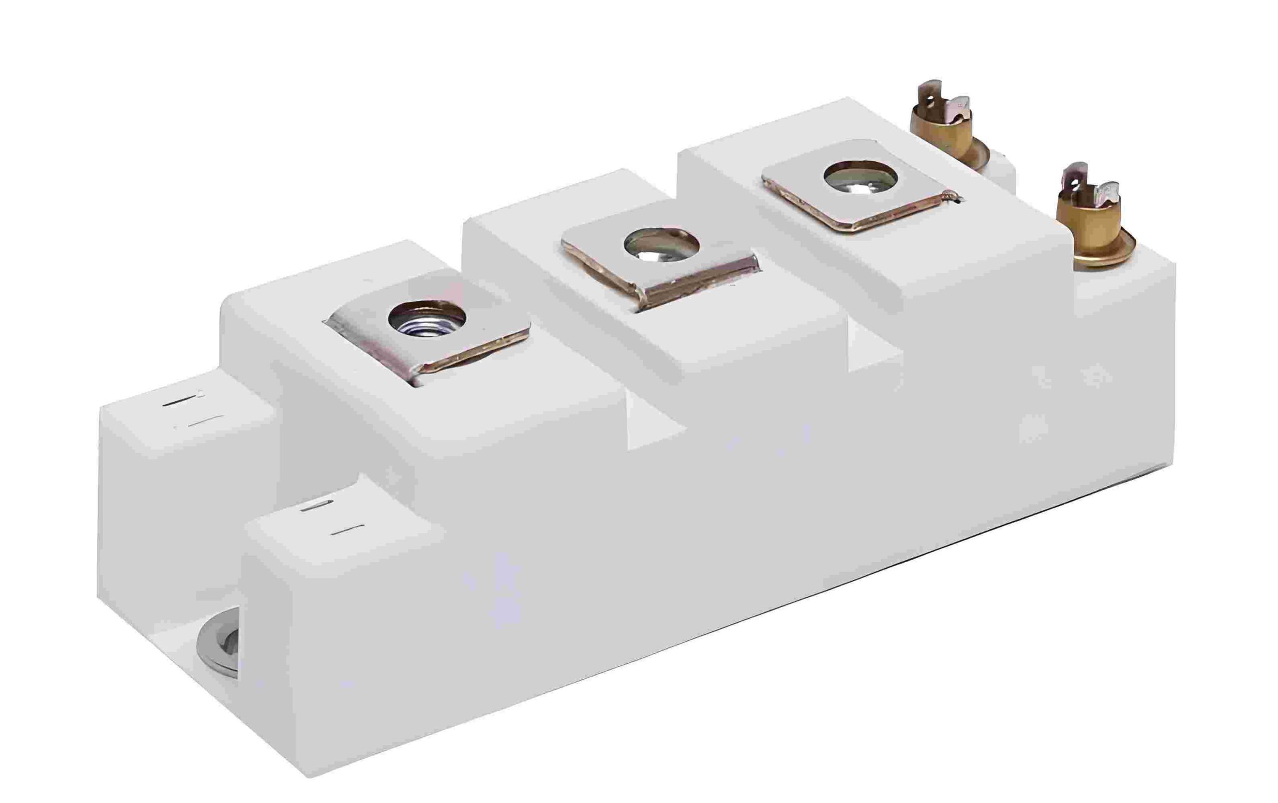
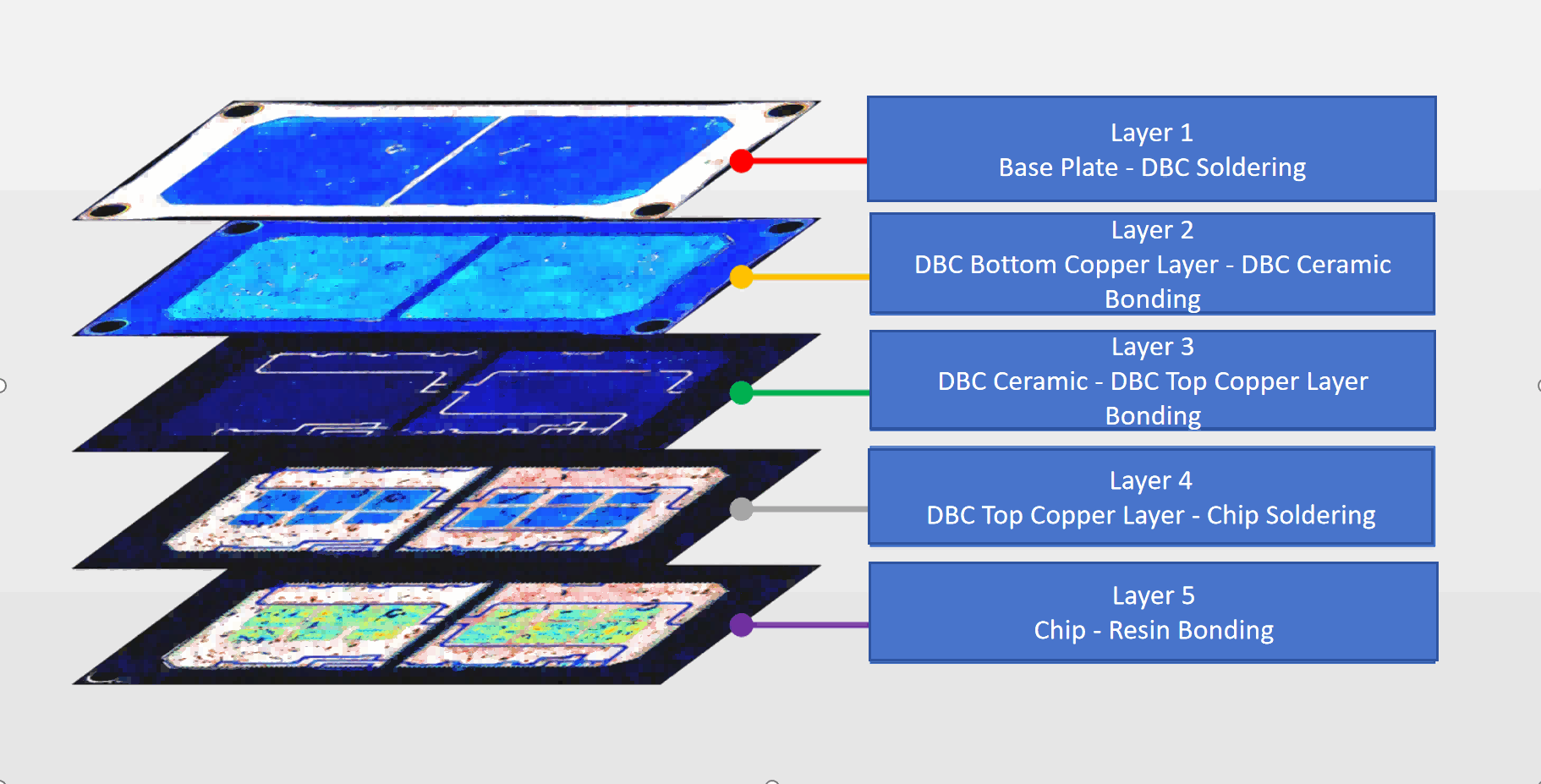
As core power devices in fields such as new energy vehicles and photovoltaic inverters, IGBT modules contain multiple complex layers (such as chips, solder layers, D……
As core power devices in fields such as new energy vehicles and photovoltaic inverters, IGBT modules contain multiple complex layers (such as chips, solder layers, DBC ceramic substrates, etc.). Any minor packaging defects (such as voids in the solder layer, cracks, delamination, poor soldering, etc.) can lead to inadequate heat dissipation and concentrated thermal stress, ultimately resulting in module failure. For example, delamination defects between the IGBT chip and the heat sink baseplate may create thermal reflection surfaces, causing the chip to overheat and reducing its lifespan.
Technical Principles and Advantages of Scanning Acoustic Microscopy
Applications in IGBT Modules
During the IGBT packaging process, scanning acoustic microscopy is used for real-time quality monitoring at critical stages:
Post-Reflow Soldering:Inspect the uniformity of the solder layers to ensure consistent bonding and thermal performance.
Pre-Molding Encapsulation:Verify the integrity of internal structures before encapsulation to prevent defect propagation during subsequent manufacturing steps.
Reliability Assessment:Evaluate the long-term reliability of the modules by analyzing the distribution and area ratio of internal defects. This involves combining defect detection data with thermal cycling test results to predict product lifespan and provide a basis for reliability assessments.
Delamination:Detect interface separations between the DBC ceramic substrate and the solder layer, which can lead to thermal mismatches and failure over time.
Voids:Identify air pockets or unfilled regions within the solder layers that can compromise thermal conductivity and structural integrity.
Cracks:Detect fractures in chip bonding wires or solder layers, which can result from mechanical stress or thermal cycling.
Poor Soldering (Cold Solder Joints):Identify incomplete bonding at interfaces, which can lead to electrical and thermal performance issues.
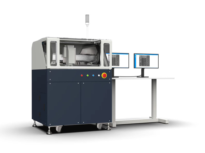
Taking the Hiwave S600 as examples
Multi-mode Scanning:Support for A-scan, B-scan, C-scan, T-scan, and tomographic scanning with a resolution of up to 0.1 μm. This versatility allows for detailed inspection of various internal structures within IGBT modules.
Automated Analysis:Automatic defect area calculation and report generation, streamlining the inspection process and reducing human error.
Integration with Manufacturing Execution Systems (MES) for digitalized data management, ensuring seamless data flow and enhanced traceability.
Wide Application:
Successfully deployed in leading companies such as BYD and Huawei, TATA Group covering a broad range of inspection scenarios including automotive IGBT modules and water-cooled plate welding.
These systems have proven their effectiveness in diverse applications, providing reliable quality assurance for critical components in new energy vehicles and other advanced technologies.
International Equipment Comparison
PVA TePla and KSI (Germany) are well-known for their advanced ultrasonic scanning technologies, delivering high precision and reliability.
Sonix (USA) is recognized for its high-resolution equipment, such as the V-400E model, which sets industry standards for quality and performance.
Hiwave(China) offerings represent a balance between advanced technology and affordability, making them competitive choices in the global market.
Future Development Trends
As IGBT modules advance towards higher power density, ultrasonic scanning technology is evolving in these key areas:
Intelligence and Automation:Using AI algorithms for automatic defect classification and early warnings, improving inspection efficiency and accuracy.
Higher Resolution:Employing higher frequency probes (like 110 MHz) to better detect micron-level defects, enhancing precision.
Standardized Processes:Promoting industry standards (such as IPC/JEDEC) to make inspection results more comparable and reliable across different manufacturers.
In summary, ultrasonic scanning microscopes provide high-precision, non-destructive testing, making them essential for quality control in IGBT modules. This is especially important in high-reliability fields like new energy vehicles, where their application will continue to grow and deepen.