Non-Destructive Void Rate Inspection for DBC and AMB Ceramic Substrates
views:368
author:Hiwave
source:Hiwave
time:2025-10-10
catogory:News
With the rapid development of new energy, electric vehicles, 5G communications and other industries, the demand for semiconductor power devices such as IGBTs is also……
With the rapid development of new energy, electric vehicles, 5G communications and other industries, the demand for semiconductor power devices such as IGBTs is also rapidly increasing, and performance requirements are becoming higher and higher.
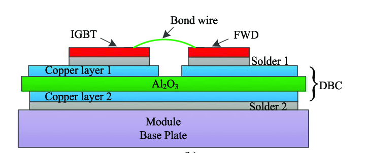
Direct Bonded Copper (DBC) substrate is a composite substrate made by bonding copper foil to ceramic surfaces such as alumina (Al₂O₃) and aluminum nitride (AlN) at high temperature through a thermal fusion bonding process. The Active Metal Brazing (AMB) substrate process is a further development of DBC technology. AMB substrates achieve bonding through a chemical reaction between the ceramic and active metal brazing paste at high temperature, resulting in higher bonding strength and better reliability. Therefore, this process is more suitable for manufacturing ceramic substrates used in IGBT module packaging for electric vehicles and locomotives. To ensure the reliability and safety of subsequent IGBT modules and other components, ultrasonic scanning acoustic microscopy must be used to inspect the internal bonding layers of DBC and AMB substrates for voids and delamination. Only DBC and AMB substrates that pass Scanning Acoustic Microscopy inspection will be used in the manufacture of power modules.
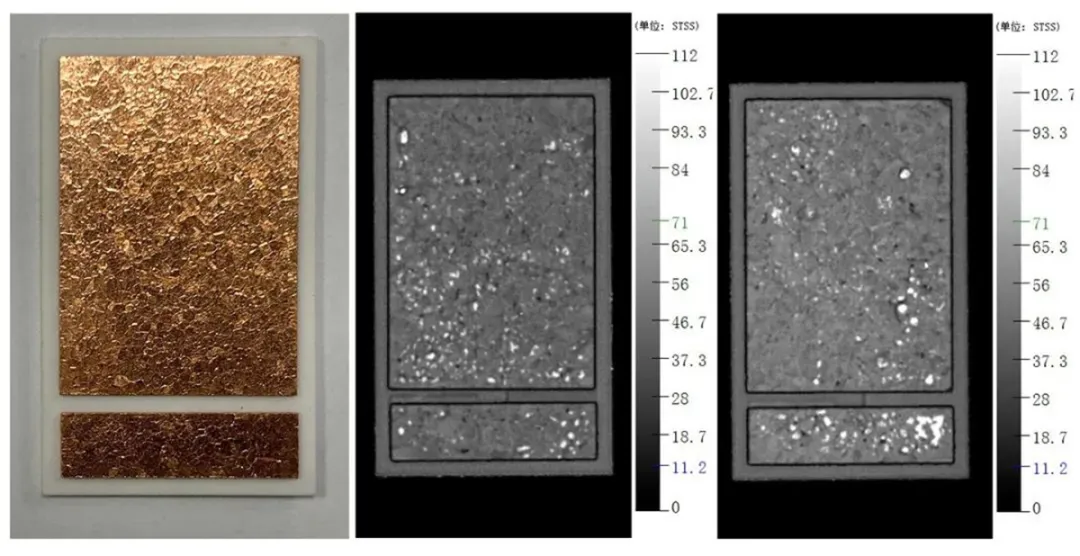
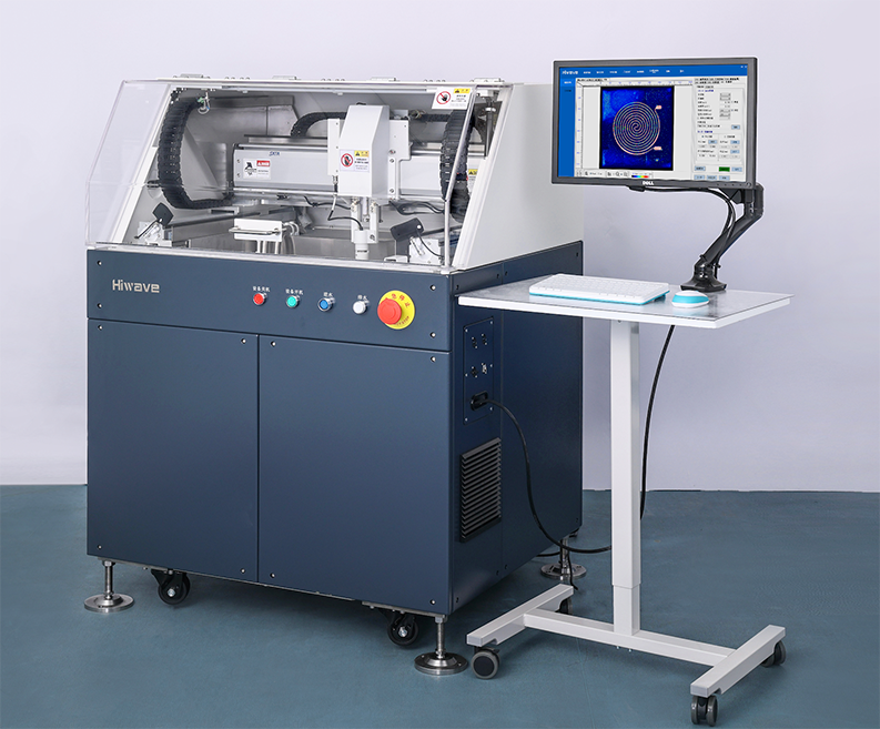
The IGBT module is composed of a baseplate, direct bonded copper (DBC) or active metal brazed (AMB) ceramic substrates, semiconductor chips, and other components. The welding quality between these layers directly affects the reliability of IGBT and other power modules. Scanning Acoustic Microscopy (SAM), also known as Scanning Acoustic Microscope or C-SAM machine, utilizes ultrasonic signals to perform non-destructive inspection of bonding interfaces and filler layers within the sample. It can effectively detect and analyze defect rates, making it an essential tool for quality control and failure analysis in semiconductor packaging.
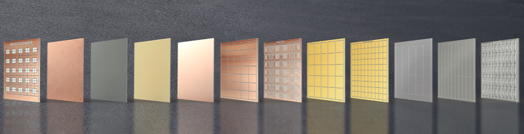
The DBC/AMB ceramic substrate employs surface metallization technology and has a three-layer structure: a ceramic insulating layer in the middle, with copper layers bonded on both top and bottom surfaces. The top copper layer is etched with circuit patterns for electrical conduction, while the bottom copper layer is directly soldered to the heat sink for thermal dissipation and does not require circuit patterning. For IGBT and other power modules, internal insulation and thermal conductivity of the DBC/AMB substrate are critical performance indicators. SAM can effectively detect internal defects such as voids, delamination, and cracks in DBC/AMB substrates, enabling effective screening of good units and ensuring high yield and product quality.
Typically, the surface of a DBC/AMB substrate features complex and fine “island-like” circuit patterns, with hundreds of individual metal islands on a single panel. To achieve full, non-destructive inspection of all units, ultrasonic scanning acoustic microscopy plays an irreplaceable role by enabling fast, efficient, high-resolution, and non-destructive testing.
Scanning Acoustic Microscopy (SAM) is a critical non-destructive testing tool for detecting internal defects in ceramic substrates such as Direct Bonded Copper (DBC) and Active Metal Brazing (AMB). By transmitting high-frequency ultrasound through the material and analyzing the reflected signals at interfaces, SAM can precisely identify internal defects such as voids, delamination, cracks, and unbonded areas—especially at the bonding interface between copper and ceramic materials like Al₂O₃, AlN, and Si₃N₄. With advantages including micron-level resolution, non-destructiveness, and the ability to perform layer-by-layer imaging, SAM enables fast, automated scanning of large-area, multi-unit substrates. It is widely used in incoming inspection, process optimization, and failure analysis of high-reliability electronic devices such as IGBT and SiC power modules, ensuring long-term stable operation under high temperature, high humidity, and high power cycling conditions.
Ceramic substrates (DBC/AMB) are key materials in PCB manufacturing, and their quality directly impacts circuit performance and product reliability. To ensure stability in high-power and high-frequency applications, accurate internal defect detection is essential. Hiwave Ultrasonic offers professional Scanning Acoustic Microscopy (SAM) testing services, providing customized, efficient solutions for DBC and AMB substrate inspection. Samples are welcome—We will deliver detailed analysis reports to support quality improvement and process optimization.