What defects does Scanning Acoustic Microscope (SAM) detect?
views:1,342
author:admin
source:Hiwave
time:2024-12-25
catogory:Frequently Asked Questions
A Scanning Acoustic Microscope (SAM/SAT ), which utilizes ultrasound for defect detection and failure analysis, is a non-contact, non-destructive testing tool that ……
A Scanning Acoustic Microscope (SAM/SAT ), which utilizes ultrasound for defect detection and failure analysis, is a non-contact, non-destructive testing tool that is equally important alongside devices like infrared cameras and X-ray equipment. It is widely used in process control and scientific research. So, what kinds of defects can a scanning acoustic microscope detect in materials/devices?
1.Detection of Impurity Particle Defects by SAM/SAT
Due to the complex processes involved in semiconductor manufacturing, it’s common for particle impurities to appear inside the products. The industry has very strict standards for these impurities, as exceeding these standards can significantly impact product quality. SAM/SAT can accurately detect the quantity and distribution of impurities, ensuring that the quality of the product meets the required standards.
2.Detection of Internal Crack Defects by SAM/SAT
In precision-made electrical components or semiconductor products, internal cracks are a frequent quality issue. SAM/SAT can detect minute cracks within the product by utilizing the impedance of ultrasound, effectively screening out products with internal cracks to prevent defective items from entering the market.
3.Detection of Delamination Defects by SAM/SAT
Delamination defects are also commonly found in semiconductors and electronic components. Traditional ultrasonic testing equipment has historically lacked precision in detecting delamination defects. However, the emergence of SAM/SAT has filled this gap, offering extremely high accuracy in delamination defect detection.
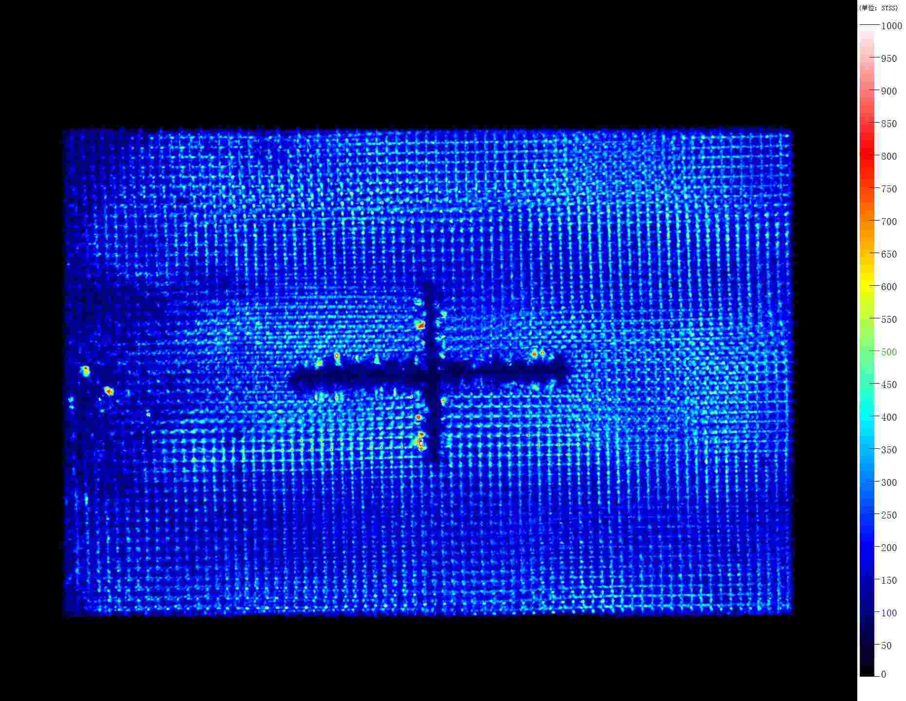
4.Detection of Voids and Porosity by SAM/SAT
SAM/SAT can identify voids and porosity in weld points, adhesives, or encapsulation materials, which could affect electrical performance and thermal conductivity efficiency. For multi-layer printed circuit boards (PCBs), SAM/SAT can detect tiny air bubbles between layers, which is crucial for ensuring the reliability and durability of the PCBs.
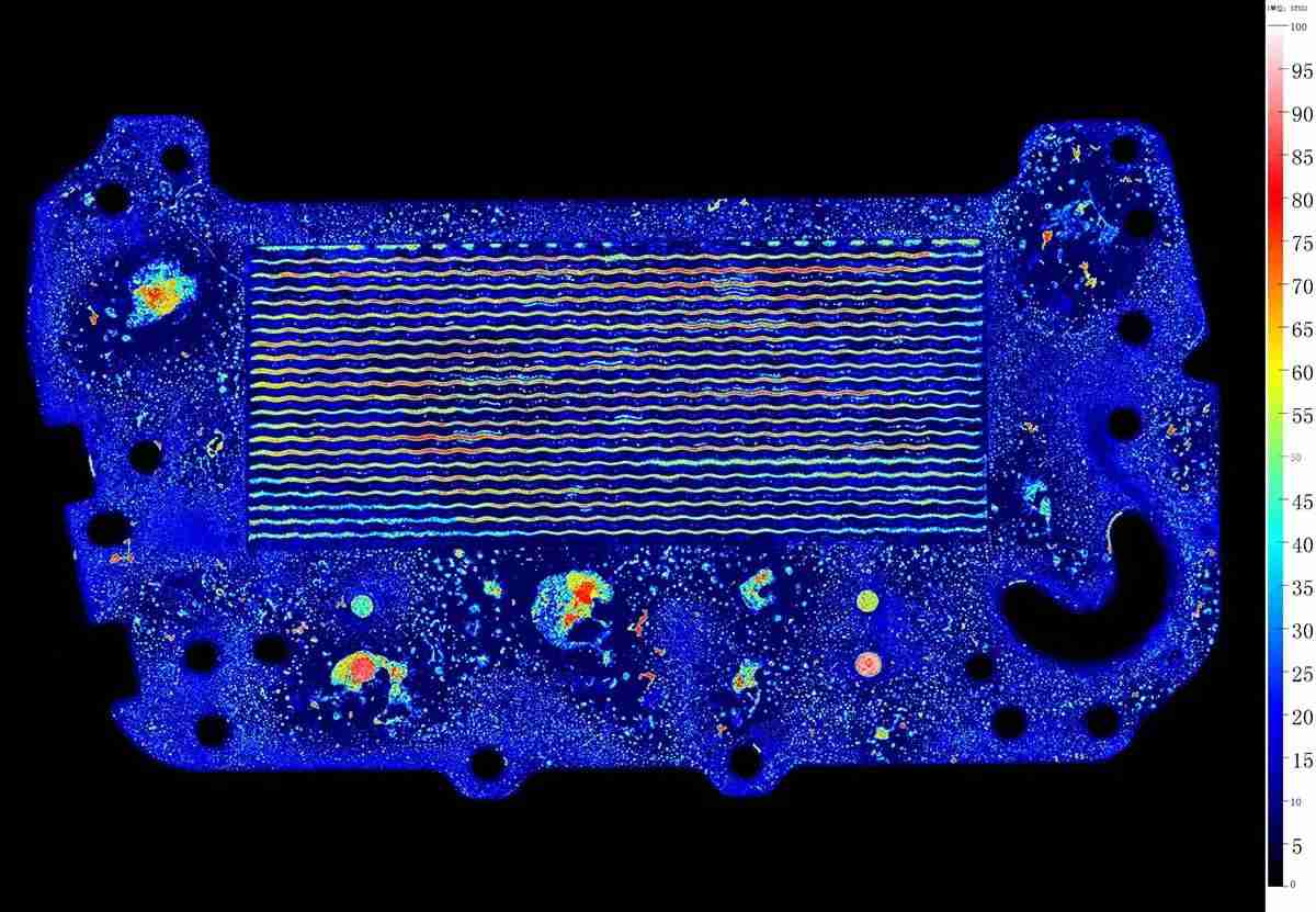
5.Inspection of Welding Quality by SAM/SAT
SAM/SAT can check the quality of weld points, including issues like incomplete solder joints (cold solder), bridging, and other welding defects. Ensuring the quality of these welds is crucial for maintaining the long-term stability of electronic products. It can be used to evaluate the soldering effectiveness of SMT (Surface Mount Technology) components.
6.Internal Structure Inspection by SAM/SAT
For complex structures such as integrated circuits and MEMS (Micro-Electro-Mechanical Systems), SAM/SAT enables non-destructive internal viewing, helping engineers understand their internal construction. This aids in studying the microstructure of new materials, providing data support for the development of new materials.
7.Packaging Inspection by SAM/SAT
SAM/SAT ensures that packaging has no cracks or other defects that could compromise its seal, which is vital for preventing moisture ingress and protecting sensitive components from environmental damage. This type of inspection is especially critical for high-reliability applications such as medical devices and military equipment.
8.Application in Failure Analysis by SAM/SAT
When a product fails, SAM/SAT can help pinpoint the source of the failure, determining whether it’s due to design flaws or issues during the manufacturing process. By comparing normal and faulty SAM/SAT ples, it accelerates the identification of root causes and suggests corrective actions.
The Scanning Acoustic Microscope (SAM/SAT) can be applied to non-destructive testing and visualization analysis of various defects such as internal damage and discontinuities in semiconductor device packages like QFN, BGA, FlipChip, CSP, MCM, etc. Additionally, it supports non-destructive internal inspection of MEMS, manufacturing process analysis, and characteristic analysis of materials such as ceramics, glass, metals, plastics, and more.