Why Traditional Microscopes Fail in Detecting Micro-Cracks in PCBs
views:583
author:admin
source:Hiwave
time:2025-02-06
catogory:Frequently Asked Questions
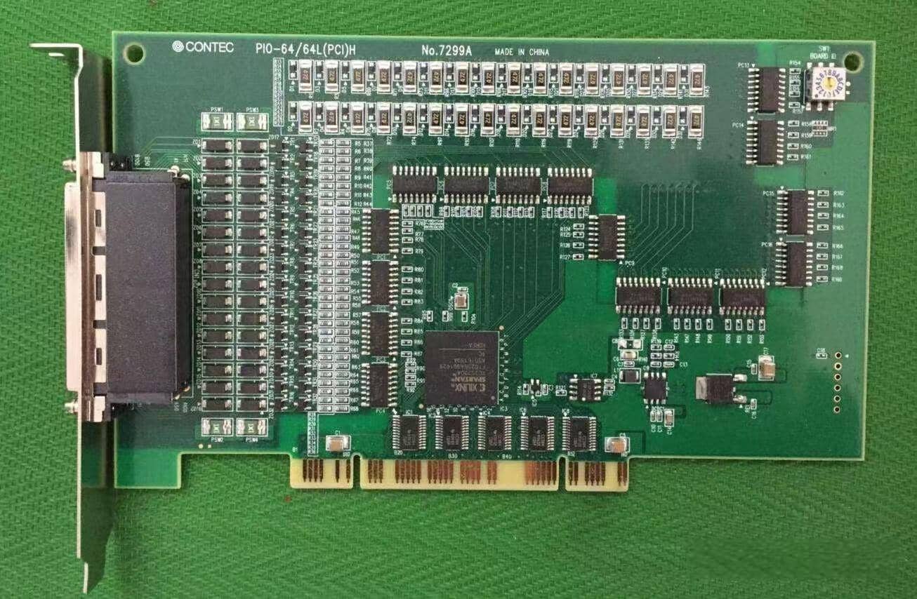
In the electronics manufacturing industry, the quality of printed circuit boards (PCBs) directly affects the performance and reliability of products. Micro-cracks ar……
In the electronics manufacturing industry, the quality of printed circuit boards (PCBs) directly affects the performance and reliability of products. Micro-cracks are one of the common defects in PCB manufacturing, often caused by thermal stress, mechanical stress, or material non-uniformity. Although traditional microscopes perform excellently in surface defect detection, they often fall short when it comes to detecting micro-cracks in PCBs. This article will explore the limitations of traditional microscopes and introduce how ultrasonic scanning microscopes can serve as an ideal tool for addressing this issue.
Limitations of Traditional Microscopes
Limitations of Surface Detection
Traditional microscopes, such as optical microscopes, are primarily used for observing the surface of samples. However, micro-cracks in PCBs are often located inside the material or beneath the surface. These cracks can be extremely small (typically at the micrometer level) and covered by multiple layers, making it impossible for traditional microscopes to penetrate the surface layer for effective detection.
Resolution Limitations
Even at high magnifications, the resolution of traditional microscopes is limited by the optical diffraction limit, making it difficult to clearly capture the details of micro-cracks. Additionally, optical microscopes require high reflectivity and contrast on the sample surface, and the complexity of PCB materials may result in blurred or distorted images.
Inability to Achieve Non-Destructive Testing
Traditional microscopes typically require cutting or polishing of samples to observe internal structures. This destructive testing method is not only time-consuming but also alters the original state of the sample, potentially leading to inaccurate detection results.
Advantages of Ultrasonic Scanning Microscopes
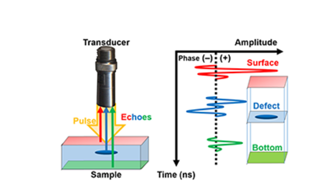
Ultrasonic scanning microscopes (C-Scan) utilize high-frequency ultrasonic waves to penetrate materials, enabling the detection of internal defects without damaging the sample. Below are the core advantages of using ultrasonic scanning microscopes for detecting micro-cracks in PCBs:
High-Resolution Imaging
Ultrasonic scanning microscopes can achieve a resolution of up to 0.1 micrometers, allowing for clear capture of micro-cracks and their propagation paths within PCBs. With 3D imaging technology, users can intuitively observe the depth, length, and shape of cracks.
Multi-Layer Material Penetration Capability
Ultrasonic waves can penetrate the multi-layer structure of PCBs, detecting defects hidden beneath the surface. Whether it’s inner-layer cracks or solder joint defects, ultrasonic scanning microscopes provide accurate detection results.
Non-Destructive Testing
Ultrasonic scanning microscopes do not require cutting or polishing of samples, completely avoiding the issues associated with destructive testing. This is particularly important for applications that require preserving the integrity of the sample, such as research and development and quality control.
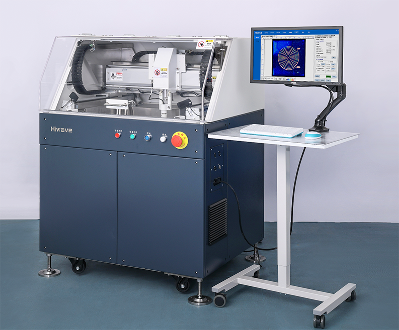
Automation and Efficiency
Modern ultrasonic scanning microscopes are typically equipped with automated scanning systems and intelligent analysis software, enabling rapid completion of large-area inspections and automatic generation of inspection reports. This significantly improves detection efficiency and reduces human operation errors.
The limitations of traditional microscopes in detecting micro-cracks in PCBs are evident, while ultrasonic scanning microscopes, with their high resolution, multi-layer penetration capabilities, and non-destructive testing features, have emerged as the ideal tool for addressing this issue. For electronics manufacturing companies, investing in ultrasonic scanning microscopes is not only crucial for improving product quality but also a significant step towards enhancing market competitiveness.